Epson Research and Development
Page 37
Vancouver Design Center
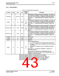
5.2.3 LCD Interface
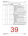
Table 5-3: LCD Interface Pin Descriptions
RESET#
State
Pin Name
Type
Pin #
Cell
Description
Panel data bus. Not all pins are used for some panels - see Table 5-9:,
“LCD Interface Pin Mapping,” on page 42 for details. Unused pins are
driven low. FPDAT[15:8] can be configured for MediaPlug interface -
see Table 5-11:, “MediaPlug Interface Pin Mapping,” on page 43 for
details.
FPDAT[8:0]
O
88, 86-79
CN3
CN3D
C/TS3U
CN3
0
Panel data bus. Not all pins are used for some panels - see Table 5-9:,
“LCD Interface Pin Mapping,” on page 42 for details. Unused pins are
driven low. FPDAT[15:8] can be configured for MediaPlug interface -
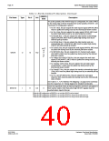
0a
or
FPDAT9
O
IO
O
89
Hi-Zb see Table 5-11:, “MediaPlug Interface Pin Mapping,” on page 43 for
details.
Panel data bus. Not all pins are used for some panels - see Table 5-9:,
“LCD Interface Pin Mapping,” on page 42 for details. Unused pins are
0c
or
FPDAT[13:10]
FPDAT[15:14]
93-90
95,94
driven low. FPDAT[15:8] can be configured for MediaPlug interface -
Hi-Zd see Table 5-11:, “MediaPlug Interface Pin Mapping,” on page 43 for
details.
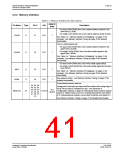
Panel data bus. Not all pins are used for some panels - see Table 5-9:,
“LCD Interface Pin Mapping,” on page 42 for details. Unused pins are
driven low. FPDAT[15:8] can be configured for MediaPlug interface -
see Table 5-11:, “MediaPlug Interface Pin Mapping,” on page 43 for
details.
0
FPFRAME
FPLINE
O
O
O
73
74
77
CN3
CN3
CO3
0
0
0
Frame pulse
Line pulse
FPSHIFT
Shift clock
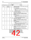
This is a multi-purpose pin:
• For TFT/D-TFD panels this is the display enable output (DRDY).
• For passive LCD with Format 1 interface this is the 2nd Shift Clock
(FPSHIFT2).
0e
or
1f
• For all other LCD panels this is the LCD backplane bias signal
(MOD).
DRDY
O
76
CO3
See Table 5-9:, “LCD Interface Pin Mapping,” on page 42 and
REG[030h] for details.
This pin can also be configured as the MediaPlug power pin
VMPEPWR - see Table 5-10:, “MA11, MA10, MA9, and DRDY Pin
Mapping,” on page 43 for details.
a
When the MD configuration at RESET# is set such that FPDAT9 is used as FPDAT9.
When the MD configuration at RESET# is set such that FPDAT9 is used as VMPRCTL.
b
c
When the MD configuration at RESET# is set such that FPDAT[13:10] is used as FPDAT[13:10].
d
e
When the MD configuration at RESET# is set such that FPDAT[13:10] is used as VMPD[3:0].
When the MD configuration at RESET# is set such that DRDY is used as DRDY (MOD).
When the MD configuration at RESET# is set such that DRDY is used as VMPEPWR.
f
Hardware Functional Specification
Issue Date: 01/02/06
S1D13506
X25B-A-001-10

 EPSON [ EPSON COMPANY ]