Epson Research and Development
Page 35
Vancouver Design Center
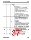
5.2.2 Memory Interface
Table 5-2: Memory Interface Pin Descriptions
RESET#
State
Pin Name
Type
Pin #
Cell
Description
• For dual-CAS# DRAM, this is the column address strobe for the
lower byte (LCAS#).
• For single-CAS DRAM, this is the column address strobe (CAS#).
LCAS#
O
51
CO1
1
See Table 5-8:, “Memory Interface Pin Mapping,” on page 41 for
summary. See Memory Interface Timing on page 70 for detailed
functionality.
This is a multi-purpose pin:
• For dual-CAS# DRAM, this is the column address strobe for the
upper byte (UCAS#).
• For single-CAS# DRAM, this is the write enable signal for the
upper byte (UWE#).
UCAS#
O
52
CO1
1
See Table 5-8:, “Memory Interface Pin Mapping,” on page 41 for
summary. See Memory Interface Timing on page 70 for detailed
functionality.
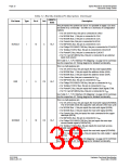
• For dual-CAS# DRAM, this is the write enable signal (WE#).
• For single-CAS# DRAM, this is the write enable signal for the lower
byte (LWE#).
WE#
O
O
53
54
CO1
CO1
1
1
See Table 5-8:, “Memory Interface Pin Mapping,” on page 41 for
summary. See Memory Interface Timing on page 70 for detailed
functionality.
Row address strobe - see Memory Interface Timing on page 70 for
detailed functionality.
RAS#
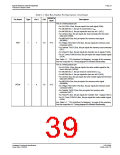
Bi-directional memory data bus.
34, 36, 38,
40, 42, 44,
46, 48, 49,
47, 45, 43,
41, 39, 37,
35
During reset, these pins are inputs and their states at the rising edge of
RESET# are used to configure the chip - see Summary of
Configuration Options on page 39. Internal pull-down resistors (typical
values of 100KΩ/180ΚΩ at 5V/3.3V respectively) pull the reset states
to 0. External pull-up resistors can be used to pull the reset states to 1.
Hi-Z
(pull 0)
MD[15:0]
IO
C/TS1D
See Memory Interface Timing on page 70 for detailed functionality.
Hardware Functional Specification
Issue Date: 01/02/06
S1D13506
X25B-A-001-10

 EPSON [ EPSON COMPANY ]