Epson Research and Development
Page 41
Vancouver Design Center
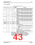
Table 5-8: Memory Interface Pin Mapping
FPM/EDO-DRAM
S1D13506
Pin Names
Sym 256Kx16
Asym 256Kx16
2-CAS# 2-WE#
D[15:0]
Sym 1Mx16
Asym 1Mx16
2-CAS# 2-WE#
2-CAS#
2-WE#
2-CAS#
2-WE#
MD[15:0]
MA[8:0]
MA91
A[8:0]
A9
GPIO32
A9
MA101
MA111
UCAS#
LCAS#
WE#
GPIO12
GPIO22
A10
A11
UCAS#
LCAS#
WE#
UWE#
CAS#
LWE#
UCAS#
UWE#
CAS#
LWE#
UCAS#
LCAS#
WE#
UWE#
CAS#
LWE#
UCAS#
LCAS#
WE#
UWE#
CAS#
LWE#
LCAS#
WE#
RAS#
RAS#
Note
1. For MA9, MA10, and MA11 functionality see Table 5-10:, “MA11, MA10, MA9,
and DRDY Pin Mapping,” on page 43.
2. All GPIO pins default to input on reset and unless programmed otherwise, should be
connected to either V or IO V if not used.
SS
DD
Hardware Functional Specification
Issue Date: 01/02/06
S1D13506
X25B-A-001-10

 EPSON [ EPSON COMPANY ]