Page 38
Epson Research and Development
Vancouver Design Center
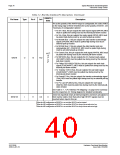
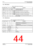
5.2.4 CRT Interface
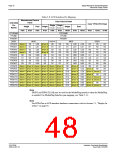
Table 5-4: CRT Interface Pin Descriptions
RESET#
State
Pin Name Type
Pin #
Cell
Description
HRTC
VRTC
O
O
107
108
CN3
CN3
0
0
Horizontal retrace signal for CRT
Vertical retrace signal for CRT
no output
current
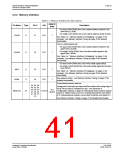
RED
GREEN
BLUE
IREF
O
O
O
I
100
103
105
101
A
A
A
A
Analog output for CRT color Red / S-Video Luminance
Analog output for CRT color Green / Composite Video Out
Analog output for CRT color Blue / S-Video Chrominance
no output
current
no output
current
Current reference for DAC. This pin must be connected to VSS if the
DAC is not needed.
--
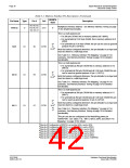
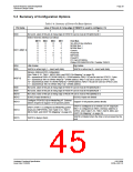
5.2.5 Miscellaneous
Table 5-5: Miscellaneous Interface Pin Descriptions
RESET#
State
Pin Name
Type
Pin #
Cell
Description
Selectable input clock. Can be used for the internal pixel clock (PCLK),
memory clock (MCLK), and MediaPlug Clock.
CLKI
I
69
C
--
Selectable input clock. Can be used for the internal pixel clock (PCLK)
and MediaPlug Clock.
CLKI2
TESTEN
VDD
I
71
70
C
CD
P
--
--
--
--
I
Test Enable. This pin should be connected to VSS for normal operation.
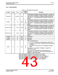
12, 33, 55,
72, 97, 109
P
P
VDD
DACVDD
99, 102, 104
P
DAC VDD
14, 32, 50,
68, 78, 87,
96, 110
VSS
P
P
P
--
VSS
DACVSS
NC
P
-
98, 106
75
--
--
DAC VSS
Not connected
S1D13506
X25B-A-001-10
Hardware Functional Specification
Issue Date: 01/02/06

 EPSON [ EPSON COMPANY ]