Page 36
Epson Research and Development
Vancouver Design Center
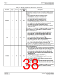
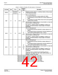
Table 5-2: Memory Interface Pin Descriptions (Continued)
RESET#
State
Pin Name
Type
Pin #
Cell
Description
58, 60, 62,
64, 66, 67,
65, 63, 61
Multiplexed memory address - see Memory Interface Timing on page
70 for detailed functionality.
MA[8:0]
O
CO1
0
This is a multi-purpose pin:
• For 2M byte DRAM, this is memory address bit 9 (MA9).
• For asymmetrical 512K byte DRAM, this is memory address bit 9
(MA9).
0a
or
• For symmetrical 512K byte DRAM, this pin can be used as general
purpose IO pin 3 (GPIO3).
MA9
IO
56
C/TS1
Hi-Zb
Note that unless configured otherwise, this pin defaults to an input and
must be driven to a valid logic level.
See Table 5-8:, “Memory Interface Pin Mapping,” on page 41 for
summary. See Memory Interface Timing on page 70 for detailed
functionality.
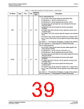
This is a multi-purpose pin:
• For asymmetrical 2M byte DRAM this is memory address bit 10
(MA10).
• For symmetrical 2M byte DRAM and all 512K byte DRAM this pin
can be used as general purpose IO pin 1 (GPIO1).
0c
or
MA10
IO
59
C/TS1
Note that unless configured otherwise, this pin defaults to an input and
must be driven to a valid logic level.
Hi-Zd
See Table 5-8:, “Memory Interface Pin Mapping,” on page 41 for
summary. See Memory Interface Timing on page 70 for detailed
functionality.
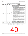
This is a multi-purpose pin:
• For asymmetrical 2M byte DRAM this is memory address bit 11
(MA11).
• For symmetrical 2M byte DRAM and all 512K byte DRAM this pin
can be used as general purpose IO pin 2 (GPIO2).
0e
or
Note that unless configured otherwise, this pin defaults to an input and
must be driven to a valid logic level.
MA11
IO
57
C/TS1
Hi-Zf
or
See Table 5-8:, “Memory Interface Pin Mapping,” on page 41 for
summary. See Memory Interface Timing on page 70 for detailed
functionality.
1g
This pin can also be configured as the MediaPlug power pin
VMPEPWR - see Table 5-10:, “MA11, MA10, MA9, and DRDY Pin
Mapping,” on page 43 for details.
a
When the MD configuration at RESET# is set such that MA9 is used as MA9.
When the MD configuration at RESET# is set such that MA9 is used as GPIO3.
When the MD configuration at RESET# is set such that MA10 is used as MA10.
When the MD configuration at RESET# is set such that MA10 is used as GPIO1.
When the MD configuration at RESET# is set such that MA11 is used as MA11.
b
c
d
e
f
When the MD configuration at RESET# is set such that MA11 is used as GPIO2.
g
When the MD configuration at RESET# is set such that MA11 is used as VMPEPWR.
S1D13506
X25B-A-001-10
Hardware Functional Specification
Issue Date: 01/02/06

 EPSON [ EPSON COMPANY ]