Page 40
Epson Research and Development
Vancouver Design Center
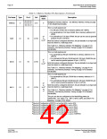
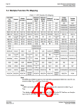
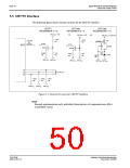
5.4 Multiple Function Pin Mapping
Table 5-7: CPU Interface Pin Mapping
S1D13506
Pin
Names
Motorola Motorola
Philips
PR31500
/PR31700
Hitachi
SH-4/SH-3
Motorola
PowerPC
Toshiba
TX3912
Generic
MIPS/ISA
MC68K
Bus 1
MC68K
Bus 2
PC Card
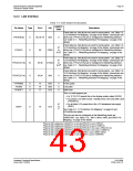
AB20
AB19
AB18
AB17
A20
A19
A18
A17
A20
A19
LatchA20
SA19
A20
A19
A18
A17
A20
A19
A11
A12
A20
A19
A18
A17
ALE
ALE
/CARDREG
CARDREG*
A18
SA18
A18
A13
/CARDIORD CARDIORD*
/CARDIOWR CARDIOWR*
A17
SA17
A17
A14
AB[16:13] A[16:13]
A[16:13]
SA[16:13] A[16:13]
A[16:13]
A[12:1]
A[15:18]
A[19:30]
A[16:13] Connected to VDD Connected to VDD
AB[12:1]
AB0
A[12:1]
A[12:1]
SA[12:1]
SA0
A[12:1]
LDS#
A[12:1]
A[12:1]
A0
A[12:1]
A0
Connected
Connected to
Connected to
A0
A31
1
1
1
to VDD
VDD
VDD
DB[15:8]
DB[7:0]
WE1#
M/R#
D[15:0]
D[7:0]
WE1#
D[15:8]
D[7:0]
WE1#
SD[15:0]
SD[7:0]
SBHE#
D[15:8]
D[7:0]
UDS#
D[31:24]
D[23:16]
DS#
D[0:7]
D[8:15]
BI
D[15:0]
D[7:0]
CE2#
D[23:16]
D[31:24]
D[23:16]
D[31:24]
/CARDxCSH CARDxCSH*
Connected to VDD Connected to VDD
Connected to VDD Connected to VDD
External Decode
External Decode
CS#
External
BUSCLK
BS#
BCLK
CKIO
BS#
CLK
CLK
CLK
AS#
CLKOUT
TS
DCLKOUT
DCLKOUT
Oscillator2
Connected
to VDD
Connected to
VDD
Connected to
VDD
AS#
Connected to VDD Connected to VDD
Connected to
VDD
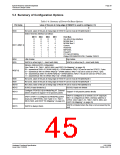
RD/WR#
RD#
RD1#
RD0#
WE0#
WAIT#
RD/WR#
RD#
R/W#
R/W#
SIZ1
SIZ0
RD/WR
TSIZ0
TSIZ1
TA
CE1#
OE#
/CARDxCSL CARDxCSL*
Connected to
VDD
MEMR#
MEMW#
/RD
/WE
RD*
WE*
Connected to
VDD
WE0#
WAIT#
WE0#
WE#
RDY#
/WAIT#
IOCHRDY DTACK# DSACK1#
inverted
WAIT#
/CARDxWAIT CARDxWAIT*
RESET# PON*
inverted
RESET
RESET# RESET# RESET#
RESET#
RESET#
RESET#
RESET
Note
All GPIO pins default to input on reset and unless programmed otherwise, must be con-
nected to either V or IO V if not used.
SS
DD
Note
1
AB0 is not used internally for these busses and must be connected to either V or
SS
V
.
DD
2
For further information on interfacing the S1D13506 to the PC Card bus, see Interfac-
ing to the PC Card Bus, document number X25B-G-005-xx.
S1D13506
X25B-A-001-10
Hardware Functional Specification
Issue Date: 01/02/06

 EPSON [ EPSON COMPANY ]