Epson Research and Development
Page 169
Vancouver Design Center
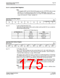
8.3.13 Look-Up Table Registers
Note
Accessing the LCD Look-Up Table (LUT) requires an active LCD PCLK and accessing
the CRT/TV LUT requires an active CRT/TV PCLK. Additionally, access to the
LUT registers is not permitted during power save mode. For further information on the
clocks, see Section 20, “Clocks” on page 224.
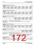
Look-Up Table Mode Register
REG[1E0h]
RW
LUT Mode Bit LUT Mode Bit
n/a
n/a
n/a
n/a
n/a
n/a
1
0
bits 1-0
Look-Up Table Mode Bits [1:0]
These bits determine which of the Look-Up Tables (LCD and CRT/TV) are accessible by
REG[1E2h] and REG[1E4h].
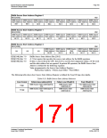
Table 8-34: LUT Mode Selection
LUT Mode Bits [1:0]
Read
LCD LUT
LCD LUT
CRT/TV LUT
Reserved
Write
LCD and CRT/TV LUT’s
LCD LUT
00
01
10
11
CRT/TV LUT
Reserved
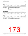
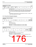
Look-Up Table Address Register
REG[1E2h]
RW
LUT Address LUT Address LUT Address LUT Address LUT Address LUT Address LUT Address LUT Address
Bit 7 Bit 6 Bit 5 Bit 4 Bit 3 Bit 2 Bit 1 Bit 0
bits 7-0
LUT Address Bits [7:0]
These 8 bits control a pointer into the Look-UpTables (LUT). The S1D13506 has three
256-position, 4-bit wide LUTs, one for each of red, green, and blue – refer to Section 12,
“Look-Up Table Architecture” on page 186 for details.
This register selects which LUT entry is read/write accessible through the LUT Data Reg-
ister (REG[1E4h]). Writing the LUT Address Register automatically sets the pointer to the
Red LUT. Accesses to the LUT Data Register automatically increment the pointer.
For example, writing a value 03h into the LUT Address Register sets the pointer to R[3].
A subsequent access to the LUT Data Register accesses R[3] and moves the pointer onto
G[3]. Subsequent accesses to the LUT Data Register move the pointer onto B[3], R[4],
G[4], B[4], R[5], etc.
Note
The RGB data is inserted into the LUT after the Blue data is written, i.e. all three colors
must be written before the LUT is updated.
Hardware Functional Specification
Issue Date: 01/02/06
S1D13506
X25B-A-001-10

 EPSON [ EPSON COMPANY ]