Epson Research and Development
Page 171
Vancouver Design Center
bit 0
Memory Controller Power Save Status
This bit indicates the power save state of the memory controller.
When this bit = 1, the memory controller is powered down and is either in self refresh or
no refresh mode.
When this bit = 0, the memory controller is powered up and is either in CBR refresh or
normal mode.
Note
When this bit reads a 1, the system may safely shut down the memory clock source.
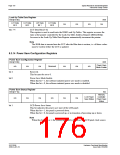
8.3.15 Miscellaneous Registers
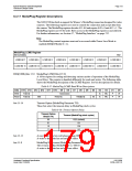
CPU-to-Memory Access Watchdog Timer Register
REG[1F4h]
RW
Mem. Access Mem. Access Mem. Access Mem. Access Mem. Access Mem. Access
n/a
n/a
Watchdog
Timer bit 5
Watchdog
Timer bit 4
Watchdog
Timer bit 3
Watchdog
Timer bit 2
Watchdog
Timer bit 1
Watchdog
Timer bit 0
bits 5-0
CPU-to-Memory Access Watchdog Timer
A non-zero value in this register enables the watchdog timer for CPU-to-memory access.
When enabled, any CPU-to-memory access cycle will be completed successfully within a
time determined by the following equation:
Maximum CPU-to-memory access cycle time = (8n + 7) × T
+ 13 × T
mclk
bclk
where:
n = A non-zero value in this register
T
= Bus clock period, or Bus clock period x 2 (if MD12 = 1, see
bclk
Table 5-6: on page 39)
= Memory clock period
T
mclk
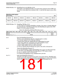
This function is required by some busses which time-out if the cycle duration exceeds a
certain time period. This function is not intended to arbitrarily shorten the
CPU-to-memory access cycle time in order gain higher CPU bandwidth. Doing so may
significantly reduce the available display refresh bandwidth which may cause display
corruption. This register does not affect CPU-to-register access or blit access.
Hardware Functional Specification
Issue Date: 01/02/06
S1D13506
X25B-A-001-10

 EPSON [ EPSON COMPANY ]