Epson Research and Development
Page 165
Vancouver Design Center
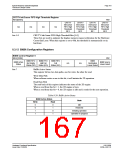
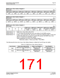
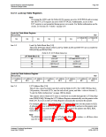
BitBlt Source Start Address Register 0
REG[104h]
RW
BitBlt Source BitBlt Source BitBlt Source BitBlt Source BitBlt Source BitBlt Source BitBlt Source BitBlt Source
Start Address Start Address Start Address Start Address Start Address Start Address Start Address Start Address
Bit 7
Bit 6
Bit 5
Bit 4
Bit 3
Bit 2
Bit 1
Bit 0
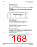
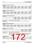
BitBlt Source Start Address Register 1
REG[105h]
RW
BitBlt Source BitBlt Source BitBlt Source BitBlt Source BitBlt Source BitBlt Source BitBlt Source BitBlt Source
Start Address Start Address Start Address Start Address Start Address Start Address Start Address Start Address
Bit 15
Bit 14
Bit 13
Bit 12
Bit 11
Bit 10
Bit 9
Bit 8
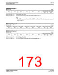
BitBlt Source Start Address Register 2
REG[106h]
RW
BitBlt Source BitBlt Source BitBlt Source BitBlt Source BitBlt Source
n/a
n/a
n/a
Start Address Start Address
Bit 20 Bit 19
Start
Bit 18
Start Address Start Address
Bit 17 Bit 16
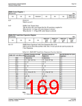
REG[104h] bits 7-0
REG[105h] bits 7-0
REG[106h] bits 4-0
BitBlt Source Start Address Bits [20:0]
A 21-bit register that specifies the source start address for the BitBlt operation.
If data is sourced from the CPU, then bit 0 is used for byte alignment within a 16-bit word
and the other address bits are ignored. In pattern fill operation, the BitBlt Source Start
Address is defined by the following equation:
Value programmed to the Source Start Address Register =
Pattern Base Address + Pattern Line Offset + Pixel Offset.
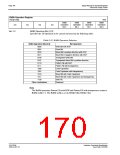
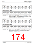
The following table shows how Source Start Address Register is defined for 8 and 16 bpp color depths.
Table 8-33: BitBlt Source Start Address Selection
Color Format
Pattern Base Address[20:0]
Pattern Line Offset[2:0]
Pixel Offset[3:0]
BitBlt Source Start Address[20:6],
BitBlt Source Start
Address[5:3]
1’b0, BitBlt Source Start
8 bpp
6’b0
Address[2:0]
BitBlt Source Start Address[20:7],
BitBlt Source Start
Address[6:4]
BitBlt Source Start
Address[3:0]
16 bpp
7’b0
Hardware Functional Specification
Issue Date: 01/02/06
S1D13506
X25B-A-001-10

 EPSON [ EPSON COMPANY ]