Page 170
Epson Research and Development
Vancouver Design Center
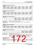
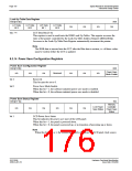
Look-Up Table Data Register
REG[1E4h]
RW
LUT Data
Bit 3
LUT Data
Bit 2
LUT Data
Bit 1
LUT Data
Bit 0
n/a
n/a
n/a
n/a
bits 7-4
LUT Data Bits [3:0]
This register is used to read/write the RGB Look-Up Tables. This register accesses the
entry at the pointer controlled by the Look-Up Table Address Register (REG[1E2h]).
Accesses to the Look-Up Table Data Register automatically increment the pointer.
Note
The RGB data is inserted into the LUT after the Blue data is written, i.e. all three colors
must be written before the LUT is updated.
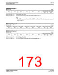
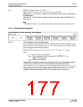
8.3.14 Power Save Configuration Registers
Power Save Configuration Register
REG[1F0h]
RW
Power Save
Mode Enable
n/a
n/a
n/a
Reserved
n/a
n/a
n/a
bit 4
bit 0
Reserved.
This bit must be set to 0.
Power Save Mode Enable
When this bit = 1, the software initiated power save mode is enabled.
When this bit = 0, the software initiated power save mode is disabled.
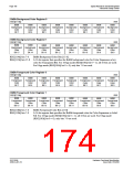
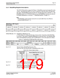
Power Save Status Register
REG[1F1h]
RO
Memory
Controller
Power Save
Status
LCD Power
Save Status
n/a
n/a
n/a
n/a
n/a
n/a
bit 1
LCD Power Save Status
This bit indicates the power save state of the LCD panel.
When this bit = 1, the panel is powered down.
When this bit = 0, the panel is powered up, or in transition of powering up or down.
Note
When this bit reads a 1, the system may safely shut down the LCD pixel clock source.
S1D13506
X25B-A-001-10
Hardware Functional Specification
Issue Date: 01/02/06

 EPSON [ EPSON COMPANY ]