Page 134
Epson Research and Development
Vancouver Design Center
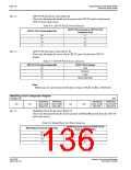
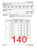
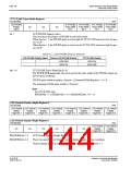
DRAM Timing Control Register 0
REG[02Ah]
RW
DRAM Timing DRAM Timing DRAM Timing DRAM Timing DRAM Timing DRAM Timing DRAM Timing DRAM Timing
Control
Register
Bit 7
Control
Register
Bit 6
Control
Register
Bit 5
Control
Register
Bit 4
Control
Register
Bit 3
Control
Register
Bit 2
Control
Register
Bit 1
Control
Register
Bit 0
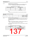
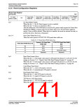
DRAM Timing Control Register 1
REG[02Bh]
RW
DRAM Timing DRAM Timing
Control
Register
Bit 9
Control
Register
Bit 8
n/a
n/a
n/a
n/a
n/a
n/a
REG[02Ah] bits 4-0
REG[02Bh] bits 1-0
DRAM Timing Control Bits [9:0]
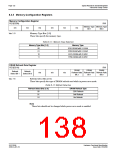
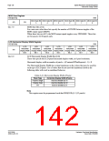
The DRAM Timing Control registers must be set based on the type of DRAM, speed of
DRAM, and MCLK frequency used. The following table provides the optimal values
for each register.
Table 8-14: DRAM Timing Control Selection
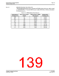
MCLK
DRAM Speed
DRAM Timing
Control Register 0
DRAM Timing
Control Register 1
Frequency
(MHz)
40
DRAM Type
(ns)
50
50
60
50
60
70
50
60
70
80
50
60
70
80
50
60
50
60
70
80
01h
01h
01h
12h
01h
00h
12h
12h
01h
00h
12h
12h
12h
01h
12h
01h
12h
12h
11h
01h
01h
01h
01h
02h
01h
00h
02h
02h
01h
01h
02h
02h
02h
01h
02h
01h
02h
02h
02h
01h
33
30
EDO
25
20
25
20
FPM
S1D13506
X25B-A-001-10
Hardware Functional Specification
Issue Date: 01/02/06

 EPSON [ EPSON COMPANY ]