Epson Research and Development
Page 133
Vancouver Design Center
bits 2-0
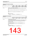
DRAM Refresh Rate Select Bits [2:0]
These bits specify the divide used to generate the DRAM refresh clock rate, which is equal
(ValueOfTheseBits + 6)
to 2
, from the MCLK source (either BUSCLK or CLKI as determined
by REG[010h] bit 0).
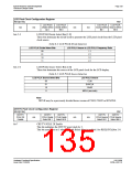
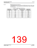
Table 8-13: DRAM Refresh Rate Selection
DRAM Refresh
Rate Bits [2:0]
MCLK Source Divide
Amount
Refresh Rate for 40MHz
MCLK Source
DRAM Refresh
Time/256 cycles
000
001
010
011
100
101
110
111
64
625 kHz
312 kHz
156 kHz
78 kHz
39 kHz
20 kHz
10 kHz
5 kHz
0.4 ms
0.8 ms
1.6 ms
3.3 ms
6.6 ms
13.1 ms
26.2 ms
52.4 ms
128
256
512
1024
2048
4096
8192
Hardware Functional Specification
Issue Date: 01/02/06
S1D13506
X25B-A-001-10

 EPSON [ EPSON COMPANY ]