Epson Research and Development
Page 129
Vancouver Design Center
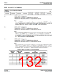
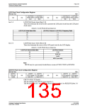
LCD Pixel Clock Configuration Register
REG[014h]
RW
LCD PCLK
Divide Select Divide Select
Bit 1 Bit 0
LCD PCLK
LCD PCLK
Source Select SourceSelect
Bit 1 Bit 0
LCD PCLK
n/a
n/a
n/a
n/a
bits 5-4
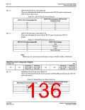
LCD PCLK Divide Select Bits [1:0]
These bits determine the divide used to generate the LCD pixel clock from the LCD pixel
clock source.
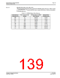
Table 8-4: LCD PCLK Divide Selection
LCD PCLK Divide Select Bits
LCD PCLK Source to LCD PCLK Frequency Ratio
00
01
10
11
1:1
2:1
3:1
4:1
bits 1-0
LCD PCLK Source Select Bits [1:0]
These bits determine the source of the LCD pixel clock for the LCD display.
Table 8-5: LCD PCLK Source Selection
LCD PCLK Source Select Bits
LCD PCLK Source
CLKI
00
01
10
11
BUSCLK
CLKI2
MCLK (see note)
Note
MCLK may be a previously divided down version of CLKI, CLKI2 or BUSCLK.
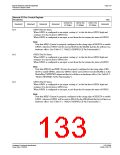
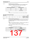
CRT/TV Pixel Clock Configuration Register
REG[018h]
RW
CRT/TV
PCLK Source PCLK Source
Select Bit 1 Select Bit 0
CRT/TV
PCLK 2X
Enable
CRT/TV
PCLK Divide PCLK Divide
Select Bit 1 Select Bit 0
CRT/TV
CRT/TV
n/a
n/a
n/a
bit 7
CRT/TV PCLK 2X Enable
This bit multiplies the CRT/TV pixel clock by 2.
This bit must be set to 1 when TV with flicker filter is enabled. See REG[1FCh] bits 2-0.
Hardware Functional Specification
Issue Date: 01/02/06
S1D13506
X25B-A-001-10

 EPSON [ EPSON COMPANY ]