Page 126
Epson Research and Development
Vancouver Design Center
8.3.2 General IO Pins Registers
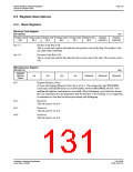
General IO Pins Configuration Register
REG[004h]
RW
GPIO3 Pin
IO Config.
GPIO2 Pin
IO Config.
GPIO1 Pin
Reserved
IO Config.
Reserved
Reserved
Reserved
Reserved
bit 3
GPIO3 Pin IO Configuration
When this bit = 1, GPIO3 is configured as an output pin.
When this bit = 0 (default), GPIO3 is configured as an input pin.
Note
Note that MD[7:6] must be properly configured at the rising edge of RESET# to enable
GPIO3, otherwise GPIO3 will be used as MA[9] for the DRAM and this bit will have no
hardware effect. (See Table 8-2: “MA[11:9]/GPIO[1:3] Pin Functionality”).
bit 2
GPIO2 Pin IO Configuration
When this bit = 1, GPIO2 is configured as an output pin.
When this bit = 0 (default), GPIO2 is configured as an input pin.
Note
Note that MD[14] and MD[7:6] must be properly configured at the rising edge of RE-
SET# to enable GPIO2, otherwise GPIO2 will be used as MA[11] for the DRAM or as
the MediaPlug VMPEPWR output and this bit will have no hardware effect. (See Table
8-2: “MA[11:9]/GPIO[1:3] Pin Functionality”).
bit 1
GPIO1 Pin IO Configuration
When this bit = 1, GPIO1 is configured as an output pin.
When this bit = 0 (default), GPIO1 is configured as an input pin.
Note
Note that MD[7:6] must be properly configured at the rising edge of RESET# to enable
GPIO1, otherwise GPIO1 will be used as MA[10] for the DRAM and this bit will have
no hardware effect. (See Table 8-2: “MA[11:9]/GPIO[1:3] Pin Functionality”).
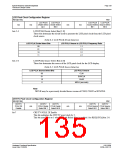
Table 8-2: MA[11:9]/GPIO[1:3] Pin Functionality
Pin
MA[10]/GPIO1
GPIO1
MD[14] on
Reset
MD[7:6] on
Reset
MA[9]/GPIO3
GPIO3
MA9
MA[11]/GPIO2
GPIO2
0
0
0
0
1
1
1
1
00
01
10
11
00
01
10
11
GPIO1
GPIO2
MA9
GPIO1
GPIO2
MA9
MA10
MA11
GPIO3
MA9
GPIO1
VMPEPWR
VMPEPWR
VMPEPWR
MA11
GPIO1
MA9
GPIO1
MA9
MA10
S1D13506
X25B-A-001-10
Hardware Functional Specification
Issue Date: 01/02/06

 EPSON [ EPSON COMPANY ]