Page 128
Epson Research and Development
Vancouver Design Center
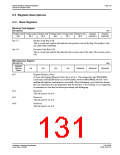
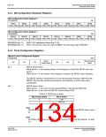
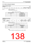
8.3.3 MD Configuration Readback Registers
MD Configuration Status Register 0
REG[00Ch]
RO
MD[7]
MD[6]
MD[5]
MD[4]
MD[3]
MD[2]
MD[1]
MD[0]
Config. Status Config. Status Config. Status Config. Status Config. Status Config. Status Config. Status Config. Status
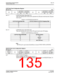
MD Configuration Status Register 1
REG[00Dh]
RO
MD[8]
MD[15]
MD[14]
MD[13]
MD[12]
MD[11]
MD[10]
MD[9]
Config. Status Config. Status Config. Status Config. Status Config. Status Config. Status Config. Status Config. Status
REG[00Ch] bits 7-0
REG[00Dh] bits 7-0
MD[15:0] Configuration Status Bits [15:0]
These read-only bits return the status of MD[15:0] at the rising edge of RESET#.
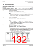
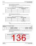
8.3.4 Clock Configuration Registers
Memory Clock Configuration Register
REG[010h]
RW
MCLK
Divide Select
MCLKSource
Select
n/a
n/a
n/a
n/a
n/a
n/a
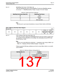
bit 4
MCLK Divide Select
When this bit = 1, the internal memory clock frequency is half of the MCLK source fre-
quency.
When this bit = 0, the memory clock frequency is equal to the MCLK source frequency.
The MCLK frequency should always be set to the maximum frequency allowed by the
DRAM. This provides maximum performance and minimizes overall system power
consumption.
bit 0
MCLK Source Select
When this bit = 1, the source for the internal MCLK is derived from BUSCLK.
When this bit = 0, the source for MCLK is derived from CLKI.
Table 8-3: MCLK Source Select
MCLK Source Select
MCLK Source
CLKI
0
1
BUSCLK
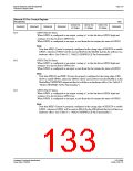
Note
The MCLK Divide Select bit must be set to 1 before changing the MCLK Source Select
bit.
Note
For further information on MCLK, refer to Section 20.2, “Clock Descriptions” on page
225.
S1D13506
X25B-A-001-10
Hardware Functional Specification
Issue Date: 01/02/06

 EPSON [ EPSON COMPANY ]