Page 124
Epson Research and Development
Vancouver Design Center
8 Registers
This section discusses how and where to access the S1D13506 registers. It also provides
detailed information about the layout and usage of each register.
8.1 Initializing the S1D13506
Before programming the S1D13506 registers, the Register/Memory Select bit
(REG[000h] bit 7) must be set.
8.1.1 Register/Memory Select Bit
At reset, the Register/Memory Select bit is set to 1. This means that only REG[000h] (read-
only) and REG[001h] are accessible until a write to REG[001h] sets bit 7 to 0 making
all registers and memory accessible. When debugging a new hardware design, this can
sometimes give the appearance that the interface is not working, so it is important to
remember to clear this bit before proceeding with debugging.
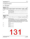
8.2 Register Mapping
The S1D13506 registers are memory-mapped. When the system decodes the input pins as
CS# = 0 and M/R# = 0, the registers may be accessed. The register space is decoded by
A20-A0.
When A20 = 1 the BitBlt data register ports are decoded allowing the system to access the
display buffer through the 2D BitBlt engine using address lines A19-A0. When A20 = 0
and A12 = 0 the registers are decoded using A8-A0 as an index. When A20 = 0 and
A12 = 1 the MediaPlug register ports are decoded using A11-A0.
The MediaPlug register ports are defined only when configuration input MD13 = 1 on reset.
When MD13 = 0 on reset, A12 is always treated as 0 and the MediaPlug register space is
not available - see Table 5-6:, “Summary of Power-On/Reset Options,” on page 39.
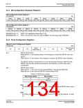
Table 8-1: “Register Mapping with CS# = 0 and M/R# = 0” shows the decoding for each
register type.
Table 8-1: Register Mapping with CS# = 0 and M/R# = 0
Register Types (Range)
BitBlt data registers (1M byte)
MediaPlug registers (4K bytes)
Main Registers (512 bytes)
Address A20-A0 Decoding
100000h to 1FFFFFh
1000h to 1FFFh
0 to 1FFh
Note
The registers may be aliased within the allocated register space. If aliasing is
undesirable, the register space must be fully decoded.
S1D13506
X25B-A-001-10
Hardware Functional Specification
Issue Date: 01/02/06

 EPSON [ EPSON COMPANY ]