Page 122
Epson Research and Development
Vancouver Design Center
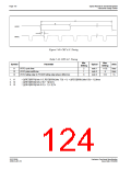
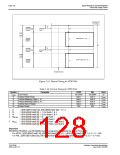
909 (NTSC)
1134 (PAL)
0
t4
Vertical
Non-Display
Period
t2
t1
Vertical
Sync
Odd
Field
1,3
Vertical
Display
Period
Odd Lines (1, 3, 5, ...)
t5
t4
Vertical
Non-Display
Period
Vertical
Sync
t3
t1
Even
Field
2,4
Vertical
Display
Period
Even Lines (2, 4, 6, ...)
Horizontal Sync
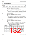
Figure 7-53: Vertical Timing for NTSC/PAL
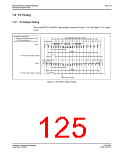
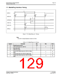
Table 7-36: Vertical Timing for NTSC/PAL
Symbol
TLINE
t1
Parameter
NTSC
PAL
63.99964
note 1
note 2
note 3
note 5
625
Units
us
Line Period
Vertical Field Period
63.55556
note 1
note 2
note 3
note 4
525
TLINE
TLINE
TLINE
TLINE
TLINE
t2
t3
t4
t5
Vertical Blanking (Fields 1, 3)
Vertical Blanking (Fields 2, 4)
Vertical Sync Position
Frame Period
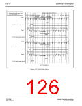
1. t1
2. t2
3. t3
= ({(REG[057] bits[1:0]), (REG[056] bits[7:0])} + 1) / 2
= ((REG[058] bits[6:0]) + 1) for fields 1 & 3
= ((REG[058] bits[6:0]) + 2) for fields 2 & 4
4. t4NTSC = ((REG[059] bits[6:0]) + 4)
= ((REG[059] bits[6:0]) + 4.5) for field 2
5. t4PAL = ((REG[059] bits[6:0]) + 5) for field 1 and field 3
= ((REG[059] bits[6:0]) + 4.5) for field 2 and field 4
for field 1
Important
REG[056], REG[057], and REG[058] must be programmed to satisfy the Frame Period (t5).
For NTSC, ({(REG[057] bits[1:0]), (REG[056] bits[7:0])} + 1) + ((REG[058] bits[6:0]) + 1) x 2 + 1) = 525
For PAL, ({(REG[057] bits[1:0]), (REG[056] bits[7:0])} + 1) + ((REG[058] bits[6:0]) + 1) x 2 + 1) = 625.
S1D13506
X25B-A-001-10
Hardware Functional Specification
Issue Date: 01/02/06

 EPSON [ EPSON COMPANY ]