DA14580
FINAL
Bluetooth Low Energy 4.2 SoC
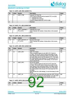
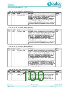
Table 127: SPI_CTRL_REG (0x50001200)
Bit
Mode Symbol
Description
Reset
6
R/W
SPI_SMN
Master/slave mode
0 = Master,
0x0
1 = Slave(SPI1 only)
5
R/W
R/W
SPI_DO
Pin SPI_DO output level when SPI is idle or when
SPI_FORCE_DO=1
0x0
0x0
4:3
SPI_CLK
Select SPI_CLK clock frequency in master mode:00 =
(XTAL) / (CLK_PER_REG *8)
01 = (XTAL) / (CLK_PER_REG *4)
10 = (XTAL) / (CLK_PER_REG *2)
11 = (XTAL) / (CLK_PER_REG *14)
2
R/W
SPI_POL
Select SPI_CLK polarity.
0 = SPI_CLK is initially low.
1 = SPI_CLK is initially high.
0x0
1
0
R/W
R/W
SPI_PHA
SPI_ON
Select SPI_CLK phase. See functional timing diagrams in
SPI chapter
0x0
0x0
0 = SPI Module switched off (power saving). Everything is
reset except SPI_CTRL_REG0 and SPI_CTRL_REG1.
When this bit is cleared the SPI will remain active in master
mode until the shift register and holding register are both
empty.
1 = SPI Module switched on. Should only be set after all con-
trol bits have their desired values. So two writes are needed!
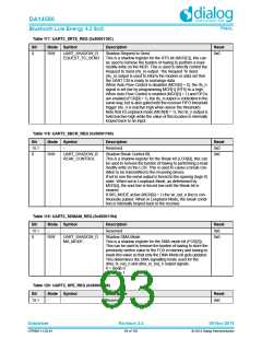
Table 128: SPI_RX_TX_REG0 (0x50001202)
Bit
Mode Symbol
R0/W SPI_DATA0
Description
Reset
15:0
Write: SPI_TX_REG0 output register 0 (TX-FIFO)
Read: SPI_RX_REG0 input register 0 (RX-FIFO)
In 8 or 9 bits mode bits 15 to 8 are not used, they contain old
data.
0x0
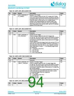
Table 129: SPI_RX_TX_REG1 (0x50001204)
Bit
Mode Symbol
R0/W SPI_DATA1
Description
Reset
15:0
Write: SPI_TX_REG1 output register 1 (MSB's of TX-FIFO)
Read: SPI_RX_REG1 input register 1 (MSB's of RX-FIFO)
In 8 or 9 or 16 bits mode bits this register is not used.
0x0
Table 130: SPI_CLEAR_INT_REG (0x50001206)
Bit
Mode Symbol
R0/W SPI_CLEAR_INT
Description
Reset
15:0
Writing any value to this register will clear the
SPI_CTRL_REG[SPI_INT_BIT]
Reading returns 0.
0x0
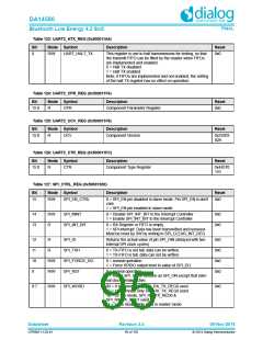
Table 131: SPI_CTRL_REG1 (0x50001208)
Bit
15:5
4
Mode Symbol
Description
Reset
0x0
-
-
Reserved
R/W
SPI_9BIT_VAL
Determines the value of the first bit in 9 bits SPI mode.
0x0
Datasheet
Revision 3.4
09-Nov-2016
CFR0011-120-01
96 of 155
© 2014 Dialog Semiconductor

 DIALOG [ Dialog Semiconductor ]