DA14580
FINAL
Bluetooth Low Energy 4.2 SoC
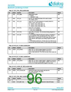
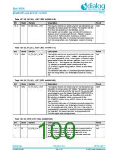
Table 137: I2C_SS_SCL_LCNT_REG (0x50001318)
Bit
Mode Symbol
R/W IC_SS_SCL_LCNT
Description
Reset
15:0
This register must be set before any I2C bus transaction can
take place to ensure proper I/O timing. This register sets the
SCL clock low period count for standard speed.
This register can be written only when the I2C interface is
disabled which corresponds to the I2C_ENABLE register
being set to 0. Writes at other times have no effect.
The minimum valid value is 8; hardware prevents values less
than this being written, and if attempted, results in 8 being
set.
0x4F
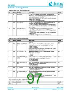
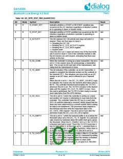
Table 138: I2C_FS_SCL_HCNT_REG (0x5000131C)
Bit
Mode Symbol
R/W IC_FS_SCL_HCNT
Description
Reset
15:0
This register must be set before any I2C bus transaction can
take place to ensure proper I/O timing. This register sets the
SCL clock high-period count for fast speed. It is used in high-
speed mode to send the Master Code and START BYTE or
General CALL. This register can be written only when the
I2C interface is disabled, which corresponds to the
I2C_ENABLE register being set to 0. Writes at other times
have no effect.
0x8
The minimum valid value is 6; hardware prevents values less
than this being written, and if attempted results in 6 being
set.
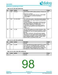
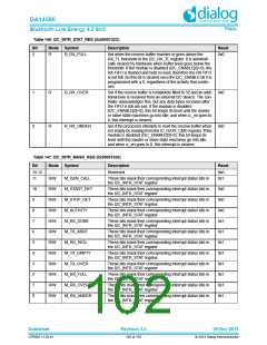
Table 139: I2C_FS_SCL_LCNT_REG (0x50001320)
Bit
Mode Symbol
R/W IC_FS_SCL_LCNT
Description
Reset
15:0
This register must be set before any I2C bus transaction can
take place to ensure proper I/O timing. This register sets the
SCL clock low-period count for fast speed. It is used in high-
speed mode to send the Master Code and START BYTE or
General CALL. This register can be written only when the
I2C interface is disabled, which corresponds to the
I2C_ENABLE register being set to 0. Writes at other times
have no effect.
0x17
The minimum valid value is 8; hardware prevents values less
than this being written, and if attempted results in 8 being
set. For designs with APB_DATA_WIDTH = 8 the order of
programming is important to ensure the correct operation of
the controller. The lower byte must be programmed first.
Then the upper byte is programmed.
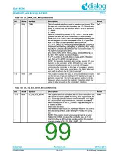
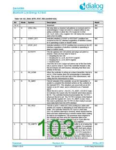
Table 140: I2C_INTR_STAT_REG (0x5000132C)
Bit
Mode Symbol
Description
Reset
0x0
15:12
11
-
-
Reserved
R
R_GEN_CALL
Set only when a General Call address is received and it is
acknowledged. It stays set until it is cleared either by dis-
abling controller or when the CPU reads bit 0 of the
I2C_CLR_GEN_CALL register. The controller stores the
received data in the Rx buffer.
0x0
Datasheet
Revision 3.4
09-Nov-2016
CFR0011-120-01
100 of 155
© 2014 Dialog Semiconductor

 DIALOG [ Dialog Semiconductor ]