DA14580
FINAL
Bluetooth Low Energy 4.2 SoC
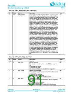
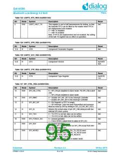
Table 123: UART2_HTX_REG (0x500011A4)
Bit
Mode Symbol
R/W UART_HALT_TX
Description
Reset
0
This register is use to halt transmissions for testing, so that
the transmit FIFO can be filled by the master when FIFOs
are implemented and enabled.
0x0
0 = Halt TX disabled
1 = Halt TX enabled
Note, if FIFOs are implemented and not enabled, the setting
of the halt TX register has no effect on operation.
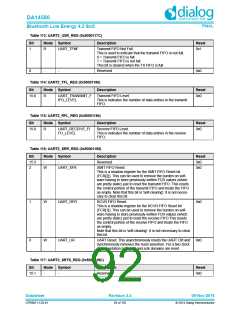
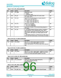
Table 124: UART2_CPR_REG (0x500011F4)
Bit
Mode Symbol
CPR
Description
Reset
15:0
R
Component Parameter Register
0x0
Table 125: UART2_UCV_REG (0x500011F8)
Bit
Mode Symbol
UCV
Description
Reset
15:0
R
Component Version
0x33303
82A
Table 126: UART2_CTR_REG (0x500011FC)
Bit
Mode Symbol
CTR
Description
Reset
15:0
R
Component Type Register
0x44570
110
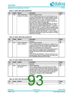
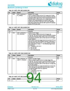
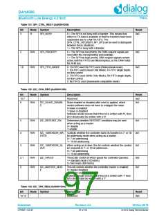
Table 127: SPI_CTRL_REG (0x50001200)
Bit
Mode Symbol
Description
Reset
15
R/W
SPI_EN_CTRL
0 = SPI_EN pin disabled in slave mode. Pin SPI_EN is don't
0x0
care.
1 = SPI_EN pin enabled in slave mode.
14
13
R/W
R
SPI_MINT
0 = Disable SPI_INT_BIT to the Interrupt Controller
1 = Enable SPI_INT_BIT to the Interrupt Controller
0x0
0x0
SPI_INT_BIT
0 = RX Register or FIFO is empty.
1 = SPI interrupt. Data has been transmitted and received-
Must be reset by SW by writing to SPI_CLEAR_INT_REG.
12
11
10
9
R
SPI_DI
Returns the actual value of pin SPI_DIN (delayed with two
internal SPI clock cycles)
0x0
0x0
0x0
0x0
R
SPI_TXH
0 = TX-FIFO is not full, data can be written.
1 = TX-FIFO is full, data can not be written.
R/W
R/W
SPI_FORCE_DO
SPI_RST
0 = normal operation
1 = Force SPIDO output level to value of SPI_DO.
0 = normal operation
1 = Reset SPI. Same function as SPI_ON except that inter-
nal clock remain active.
8:7
R/W
SPI_WORD
00 = 8 bits mode, only SPI_RX_TX_REG0 used
01 = 16 bit mode, only SPI_RX_TX_REG0 used
10 = 32 bits mode, SPI_RX_TX_REG0 &
SPI_RX_TX_REG1 used
0x0
11 = 9 bits mode. Only valid in master mode.
Datasheet
Revision 3.4
09-Nov-2016
CFR0011-120-01
95 of 155
© 2014 Dialog Semiconductor

 DIALOG [ Dialog Semiconductor ]