DA14580
FINAL
Bluetooth Low Energy 4.2 SoC
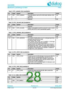
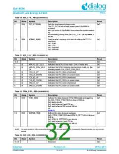
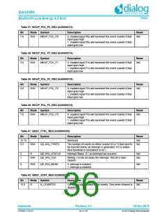
Table 20: SYS_CTRL_REG (0x50000012)
Bit
Mode Symbol
Description
Reset
2
R/W
RET_SYSRAM
Sets the development phase mode.
0x0
The PD_SYS is not actually power gated (SysRAM is
retained).
No copy action to SysRAM is done when the system wakes
up.
For emulating startup time, the OTP_COPY bit still needs to
be set.
1:0
R/W
REMAP_ADR0
Controls which memory is located at address 0x0000 for
0x0
execution.
0x0: ROM
0x1: OTP
0x2: SysRAM
0x3: RetRAM
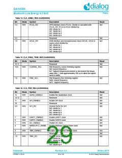
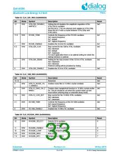
Table 21: SYS_STAT_REG (0x50000014)
Bit
15:8
7
Mode Symbol
Description
Reset
0x0
-
-
Reserved
R
R
XTAL16_SETTLED
Indicates that XTAL16 has had > 2 ms of settle time
0x0
6
XTAL16_TRIM_REA
DY
Indicates that XTAL trimming mechanism is ready, i.e. the
trimming equals CLK_FREQ_TRIM_REG.
0x1
5
4
3
2
1
0
R
R
R
R
R
R
DBG_IS_UP
Indicates that PD_DBG is functional
Indicates that PD_DBG is in power down
Indicates that PD_PER is functional
Indicates that PD_PER is in power down
Indicates that PD_RAD is functional
Indicates that PD_RAD is in power down
0x0
0x1
0x0
0x1
0x0
0x1
DBG_IS_DOWN
PER_IS_UP
PER_IS_DOWN
RAD_IS_UP
RAD_IS_DOWN
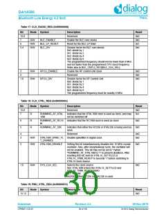
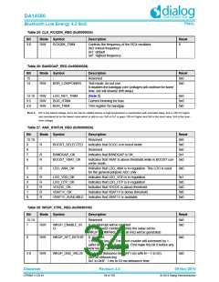
Table 22: TRIM_CTRL_REG (0x50000016)
Bit
Mode Symbol
Description
Reset
7:4
R/W
TRIM_TIME
Defines the delay between XTAL16M enable and applying
the CLK_FREQ_TRIM_REG in steps of 250 us.
0x0: apply directly
0xA
0x1: wait between 0 and 250 us
0x2: wait between 250 us and 500 us
etc.
(Note 1)
3:0
R/W
SETTLE_TIME
Defines the delay between applying
CLK_FREQ_TRIM_REG and XTAL16_SETTLED in steps of
250 us.
0x2
0x0: XTAL16_SETTLED is set direcly
0x1: wait between 0 and 250 us
0x2: wait between 250 us and 500 us
etc.
Note 1: The period duration of 250 us is derived by dividing the RC16M clock signal by 4000. Consequently, the period duration may vary over tem-
perature.
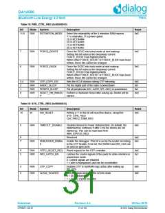
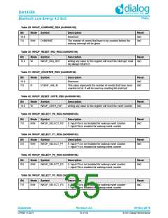
Table 23: CLK_32K_REG (0x50000020)
Bit
Mode Symbol
Description
Reset
15:13
-
-
Reserved
0x0
Datasheet
Revision 3.4
09-Nov-2016
CFR0011-120-01
32 of 155
© 2014 Dialog Semiconductor

 DIALOG [ Dialog Semiconductor ]