DA14580
FINAL
Bluetooth Low Energy 4.2 SoC
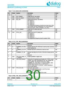
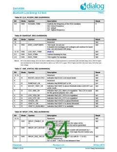
Table 25: CLK_RCX20K_REG (0x50000024)
Bit
Mode Symbol
R/W RCX20K_TRIM
Description
Reset
3:0
Controls the frequency of the RCX oscillator.
0x0: lowest frequency
8
0x7: default
0xF: highest frequency
Table 26: BANDGAP_REG (0x50000028)
Bit
15
14
Mode Symbol
Description
Reset
0x0
-
-
Reserved
R/W
BGR_LOWPOWER
Test-mode, do not use.
0x0
It disables the bandgap core (voltages will continue for some
time, but will slowely drift away)
13:10
9:5
R/W
R/W
R/W
LDO_RET_TRIM
BGR_ITRIM
(Note 2)
0x0
0x0
0x0
Current trimming for bias
Trim register for bandgap
4:0
BGR_TRIM
Note 2: 0xF is the lowest voltage, but is too low for reliable startup at high temperature in combination with extended sleep. 0xA is 100 mV higher
and considered to be the lowest value which is safe to use. 0x0 or 0x1 is again 100 mV higher and 0x0 is the reset value. 0x4 is the maxi-
mum voltage.
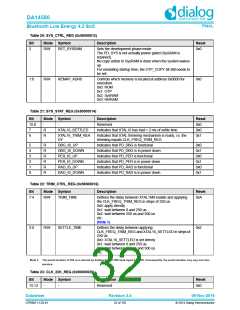
Table 27: ANA_STATUS_REG (0x5000002A)
Bit
Mode Symbol
Description
Reset
0x0
15:10
-
-
Reserved
9
8
7
6
R
-
BOOST_SELECTED
-
Indicates that DCDC is in boost mode
Reserved
0x0
0x0
R
R
BANDGAP_OK
BOOST_VBAT_OK
Indicates that BANDGAP is OK
0x1
Indicates that VBAT is above threshold while in BOOST con- 0x0
verter mode.
5
R
LDO_ANA_OK
Indicates that LDO_ANA is in regulation. This LDO is used
for the general-purpose ADC only
0x0
4
3
2
1
0
R
R
R
R
R
LDO_VDD_OK
LDO_OTP_OK
VDCDC_OK
Indicates that LDO_VDD is in regulation
Indicates that LDO_OTP is in regulation
Indicates that VDCDC is above threshold.
Indicates that VBAT1V is above threshold.
0x1
0x0
0x0
0x0
0x0
VBAT1V_OK
VBAT1V_AVAILABLE Indicates that VBAT1V is available.
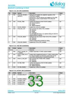
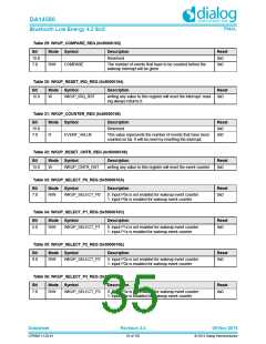
Table 28: WKUP_CTRL_REG (0x50000100)
Bit
Mode Symbol
Description
Reset
0x0
15:14
7
-
-
Reserved
R/W
WKUP_ENABLE_IR
Q
0: no interrupt will be enabled
1: if the event counter reaches the value set by
WKUP_COMPARE_REG an IRQ will be generated
0x0
6
R/W
R/W
WKUP_SFT_KEYHIT 0: no effect
1: emulate key hit. The event counter will increment by 1
0x0
(after debouncing if enabled). First make this bit 0 before any
new key hit can be sensed.
5:0
WKUP_DEB_VALUE
Keyboard debounce time (N*1 ms with N = 1 to 63).
0x0: no debouncing
0x0
0x1 to 0x3F: 1 ms to 63 ms debounce time
Datasheet
Revision 3.4
09-Nov-2016
CFR0011-120-01
34 of 155
© 2014 Dialog Semiconductor

 DIALOG [ Dialog Semiconductor ]