ES51963
4 1/2 DMM
status from STAUS pin at the falling edge of clock pulse. The content of output count is read
in order of D0, D1, ... D15 and it is read in front of the status.
Both format 1 and format 2 have two operation mode: mode 1 and mode 2. The
communication ways described above are in mode 1 at which ES51963 sends data to the
microprocessor. Mode 2 is used in the cases of the microprocessor sends control status to
ES51963 to change format, conversion rate, zero calibration, etc. The difference between
mode 1 and mode 2 is that there are a start bit and a end bit on the clock sequence for SCLK.
As ES51963 detects the start bit it enters mode 2 and receives status from STATUS. ES51963
will go back to mode 1 as it detects the end bit. There are timing restricts on the width of clock
pulse, start bit and the end bit. The communication might malfunction if the restrictions are
violated.
The communication ways and associated timing restrictions are described in detail as
follows.
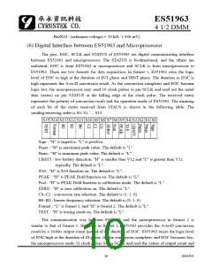
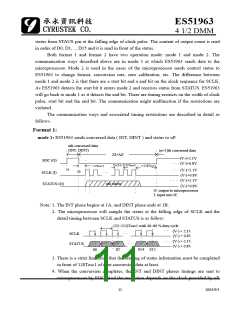
Format 1:
mode 1: ES51963 sends conversed data ( INT, DINT ) and status to uP.
nth conversed data
(INT, DINT)
(n+1)th conversed data
ZI+AZ
(V-)+2.1V
(V-)+0.8V
EOC (O)
T=(32~512)Tosc1
>=128Tosc1
>=2Tosc1
1A
(V-)+2.1V
(V-)+0.8V
(V-)+2.1V
(V-)+0.8V
1B
SCLK (I)
STATUS (O)
nth status
O: output to microprocessor
I: input into IC
Note: 1. The INT phase begins at 1A, and DINT phase ends at 1B.
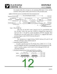
2. The microprocessor will sample the status at the falling edge of SCLK and the
detail timing between SCLK and STATUS is as follow:
(32~512)Tosc1 with 40~60 % duty cycle
(V-) + 2.1V
(V-) + 0.8V
SCLK
(V-) + 2.1V
(V-) + 0.8V
STATUS
S0
S1
S2
S14 S15
3. There is a strict limitation that the sending of status information must be completed
in front of 128Tosc1 of next conversion data at least.
4. When the conversion completes, the INT and DINT phases timings are sent to
microprocessor by EOC. And the resolution depends on the clock provided by uP.
11
2003/9/1

 CYRUSTEK [ Cyrustek corporation ]