ES51963
4 1/2 DMM
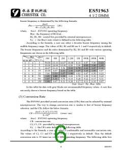
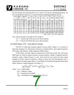
the CRs and the ratios determined by C2, C1 and C0 with various operating frequencies. An
user can decide the value of C2, C1 and C0 based on operating frequency and CR.
CRs
fosc1
6M
4M
2M 1.2M 1M 800k 600k 400k
C2 C1 C0
F2( . )
1 1 1
1 1 0
1 0 1
1 0 0
0 1 1
0 1 0
0 0 1
0 0 0
100
80
40
20
10
8
150
120
60
100
80
40
20
10*
8
50
40
30
24
25
20
20
16
15
12!
6!
10*
8
20
12!
6!
10*
5*
8
4
30
10*
5*
4!
3!
2!*
1!*
0.8!
15
3!
2.4!
1.2!
2.5*
2!*
1!*
2!*
1.6
0.8!
1.5!
1.2!
0.6! 0.4!*
12!
6!
4!
4
4!
2!*
1!*
2
3!
2!*
0.6! 0.5!* 0.4!* 0.3! 0.2!*
Unit : fosc1 : Hz , CR : times/sec
Note: About the index at the back of CR's numbers:
(1) " * " denotes that 50 Hz line noise will be rejected.
(2) " ! " denotes that 60 Hz line noise will be rejected.
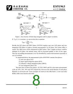
(4) Dual Slope A/D—four phases timing
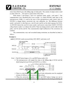
ES51963 is a dual-slope analog-to-digital converter (ADC). Figure 1 is a structure of
dual-slope integrator. Its measurement cycle has two distinct phases: input signal integration
(INT) phase and reference voltage integration (DINT) phase.
In INT phase, the input signal is integrated for a fixed time period, then A/D enters
DINT phase in which an opposite polarity constant reference voltage is integrated until the
integrator output voltage becomes to zero. Since both the time period for input signal
integration and the amount of reference voltage are fixed, thus the de-integration time is
proportional to the input signal. Hence, we can define the mathematical equation about input
signal, reference voltage integration (see Figure 1.):
TINT
1
Buf × C int
1
VIN (t)dt =
×VREF ×TDINT
∫
0
Buf × C int
where, VIN (t) = input signal
VREF = reference voltage
TINT = integration time (fixed)
TDINT = de-integration time (proportional toVIN (t) )
7
2003/9/1

 CYRUSTEK [ Cyrustek corporation ]