ES51963
4 1/2 DMM
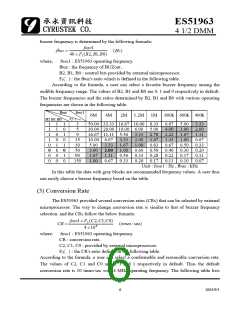
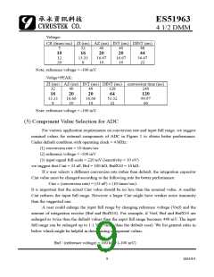
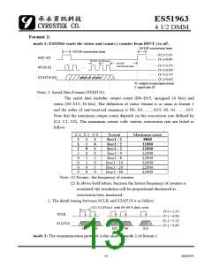
Voltage:
CR (times/sec) ZI (ms) AZ (ms) INT (ms) DINT (ms)
5
32
40
40
88
10
12
20
16
13.33
8
20
16.67
10
20
16.67
10
44
36.67
22
Note: reference voltage = -100 mV.
Voltge+PEAK:
ZI (ms) AZ (ms) INT (ms) DINT (ms) conversion time (ms)
32
40
40
128
240
16
13.33
8
20
16.66
10
20
16.66
10
64
53.32
32
120
99.97
60
Note: reference voltage = -100 mV.
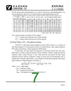
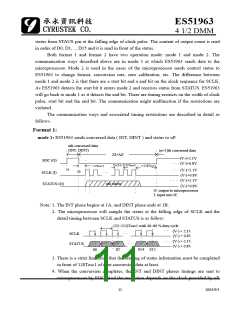
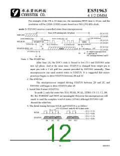
(5) Component Value Selection for ADC
For various application requirements on conversion rate and input full range, we suggest
nominal values for external components of ADC in Figure 1 to obtain better performance.
Under default condition with operating clock = 4 MHz:
(1) conversion rate = 10 times/sec
(2) reference voltage = -100 mV
(3) input signal full scale = 220 mV (sensitivity = 10 uV)
we suggest that Cint = 33 nF, Buf = 100 kΩ, BufX10 = 10 kΩ.
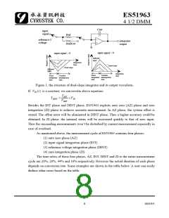
If a user selects a different conversion rate rather than default, the integration capacitor
Cint value must be changed according to the following rule for better performance:
Cint × (conversion rate) = (33 nF) × (10 times/sec).
It is important that the actual Cint value should be no less than the nominal value. A smaller
Cint reduces the input full range. However a larger Cint might have weaker noise immunity
than the suggested one.
A user could enlarge the input full range by changing reference voltage (Vref) and the
amount of integration resistor (Buf and BufX10). For example, if Vref, Buf and BufX10 are
enlarged as twice than the default values then the input full range becomes 440 mV. The input
full range can be enlarged up to 1.1 V (5 times than the default case). We list general rules in
below which might be helpful in determining component values.
Buf / (reference voltage) = 100 kΩ / (-100 mV)
9
2003/9/1

 CYRUSTEK [ Cyrustek corporation ]