U631H16
SoftStore 2K x 8 nvSRAM
Features
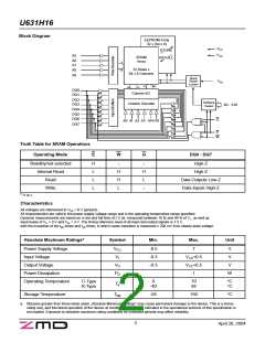
tion), or from the EEPROM to the
SRAM (the RECALL ) operation)
are initiated through software
sequences.
! Packages: PDIP28 (300 mil)
PDIP28 (600 mil)
! High-performance CMOS nonvola-
tile static RAM 2048 x 8 bits
! 25, 35 and 45 ns Access Times
! 12, 20 and 25 ns Output Enable
Access Times
SOP28 (300 mil)
SOP24 (300 mil)
The U631H16 combines the high
performance and ease of use of a
fast SRAM with nonvolatile data
integrity.
Description
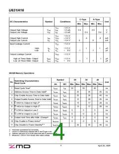
! Software STORE Initiation
(STORE Cycle Time < 10 ms)
! Automatic STORE Timing
! 105 STORE cycles to EEPROM
! 10 years data retention in
EEPROM
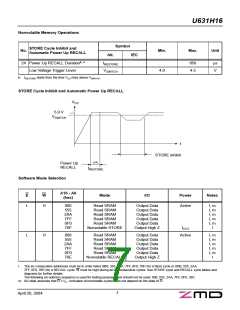
The U631H16 has two separate
modes of operation: SRAM mode
and nonvolatile mode. In SRAM
mode, the memory operates as an
ordinary static RAM. In nonvolatile
operation, data is transferred in
parallel from SRAM to EEPROM or
from EEPROM to SRAM. In this
mode SRAM functions are disab-
led.
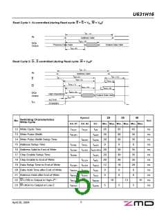
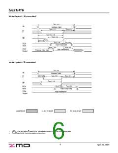
Once a STORE cycle is initiated,
further input or output are disabled
until the cycle is completed.
Because a sequence of addresses
is used for STORE initiation, it is
important that no other read or
write accesses intervene in the
sequence or the sequence will be
aborted.
! Automatic RECALL on Power Up
! Software RECALL Initiation
(RECALL Cycle Time < 20 µs)
! Unlimited RECALL cycles from
EEPROM
! Unlimited Read and Write to
SRAM
Internally, RECALL is a two step
procedure. First, the SRAM data is
The U631H16 is a fast static RAM
(25, 35, 45 ns), with a nonvolatile
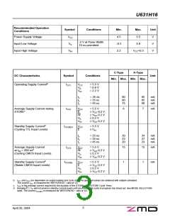
! Single 5 V ± 10 % Operation
! Operating temperature ranges:
0 to 70 °C
cleared and second, the nonvola-
tile information is transferred into
the SRAM cells.
electrically
erasable
PROM
(EEPROM) element incorporated
in each static memory cell. The
SRAM can be read and written an
unlimited number of times, while
independent nonvolatile data resi-
des in EEPROM.
-40 to 85 °C
The RECALL operation in no way
alters the data in the EEPROM
cells. The nonvolatile data can be
recalled an unlimited number of
times.
! QS 9000 Quality Standard
! ESD characterization according
! MIL STD 883C M3015.7-HBM
(classification see IC Code
Numbers)
Data transfers from the SRAM to
the EEPROM (the STORE opera-
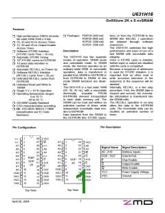
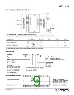
Pin Description
Pin Configuration
28
27
26
25
24
23
22
21
20
19
18
1
2
3
4
5
6
7
8
n.c.
n.c.
A7
A6
A5
A4
A3
A2
A1
VCC
W
n.c.
A8
A9
n.c.
G
1
2
3
4
5
6
7
8
A7
A6
A5
A4
A3
A2
A1
A0
DQ0
DQ1
DQ2
VSS
24
23
22
21
20
19
18
17
16
15
14
13
VCC
A8
A9
W
G
Signal Name Signal Description
A0 - A10
DQ0 - DQ7
Address Inputs
Data In/Out
PDIP
SOP
28
A10
E
SOP
24
Chip Enable
E
A10
E
Output Enable
Write Enable
Power Supply Voltage
Ground
G
W
VCC
VSS
9
DQ7
DQ6
DQ5
DQ4
DQ3
9
10
11
12
13
14
A0
DQ7
DQ6
DQ5
DQ4
DQ3
10
11
12
DQ0
DQ1
DQ2
VSS
17
16
15
Top View
Top View
1
April 20, 2004

 CYPRESS [ CYPRESS ]