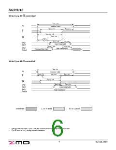
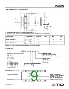
U631H16
C-Type
K-Type
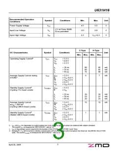
DC Characteristics
Symbol
Conditions
Unit
Min. Max. Min. Max.
VCC
IOH
IOL
= 4.5 V
=-4 mA
= 8 mA
Output High Voltage
Output Low Voltage
VOH
VOL
2.4
8
2.4
8
V
V
0.4
-4
0.4
-4
VCC
VOH
VOL
= 4.5 V
= 2.4 V
= 0.4 V
Output High Current
Output Low Current
IOH
IOL
mA
mA
Input Leakage Current
VCC
= 5.5 V
High
Low
IIH
IIL
VIH
VIL
= 5.5 V
1
1
1
1
µA
µA
=
0 V
-1
-1
-1
-1
Output Leakage Current
V
= 5.5 V
CC
High at Three-State- Output
Low at Three-State- Output
IOHZ
IOLZ
VOH
VOL
= 5.5 V
µA
µA
=
0 V
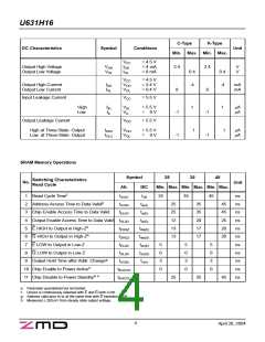
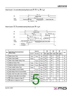
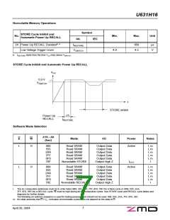
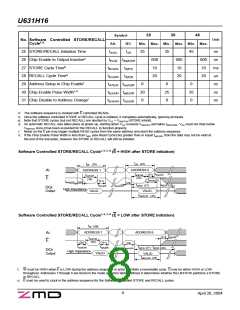
SRAM Memory Operations
Symbol
25
35
45
Switching Characteristics
No.
Unit
Read Cycle
Alt.
IEC
Min. Max. Min. Max. Min. Max.
1
2
3
4
5
6
7
8
9
Read Cycle Timef
Address Access Time to Data Validg
tAVAV
tAVQV
tELQV
tcR
25
35
45
ns
ns
ns
ns
ns
ns
ns
ns
ns
ns
ns
ta(A)
25
25
12
13
13
35
35
20
17
17
45
45
25
20
20
Chip Enable Access Time to Data Valid
ta(E)
Output Enable Access Time to Data Valid tGLQV
ta(G)
tdis(E)
tdis(G)
ten(E)
ten(G)
tv(A)
E HIGH to Output in High-Zh
G HIGH to Output in High-Zh
E LOW to Output in Low-Z
tEHQZ
tGHQZ
tELQX
5
0
3
0
5
0
3
0
5
0
3
0
G LOW to Output in Low-Z
Output Hold Time after Addr. Changeg
tGLQX
tAXQX
tELICCH
tEHICCL
19 Chip Enable to Power Activee
11 Chip Disable to Power Standbyd, e
25
35
45
e: Parameter guaranteed but not tested.
f: Device is continuously selected with E and G both LOW.
g: Address valid prior to or at the same time with E transition LOW.
h: Measured ± 200 mV from steady state output voltage.
4
April 20, 2004

 CYPRESS [ CYPRESS ]