U631H16
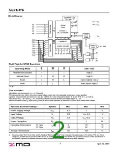
Block Diagram
EEPROM Array
32 x (64 x 8)
VCC
VSS
STORE
RECALL
A5
A6
A7
A8
A9
SRAM
Array
32 Rows x
64 x 8 Columns
Store/
Recall
Control
VCC
DQ0
DQ1
Column I/O
DQ2
DQ3
Software
Detect
Column Decoder
A0 - A10
DQ4
DQ5
DQ6
G
A0 A1 A2 A3 A4A10
DQ7
E
W
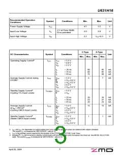
Truth Table for SRAM Operations
Operating Mode
E
W
G
DQ0 - DQ7
Standby/not selected
Internal Read
Read
H
L
L
L
High-Z
High-Z
*
*
H
H
H
L
L
Data Outputs Low-Z
Data Inputs High-Z
Write
*
* H or L
Characteristics
All voltages are referenced to VSS = 0 V (ground).
All characteristics are valid in the power supply voltage range and in the operating temperature range specified.
Dynamic measurements are based on a rise and fall time of ≤ 5 ns, measured between 10 % and 90 % of VI, as well as
input levels of VIL = 0 V and VIH = 3 V. The timing reference level of all input and output signals is 1.5 V,
with the exception of the tdis-times and ten-times, in which cases transition is measured ± 200 mV from steady-state voltage.
Absolute Maximum Ratingsa
Symbol
Min.
Max.
Unit
Power Supply Voltage
Input Voltage
VCC
VI
-0.5
-0.3
-0.3
7
V
V
VCC+0.5
VCC+0.5
1
Output Voltage
VO
PD
V
Power Dissipation
W
Operating Temperature
C-Type
K-Type
0
70
85
°C
°C
Ta
-40
Storage Temperature
Tstg
-65
150
°C
a: Stresses greater than those listed under „Absolute Maximum Ratings“ may cause permanent damage to the device. This is a stress
rating only, and functional operation of the device at condition above those indicated in the operational sections of this specification is
not implied. Exposure to absolute maximum rating conditions for extended periods may affect reliability.
2
April 20, 2004

 CYPRESS [ CYPRESS ]