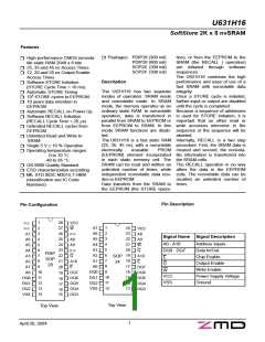
U631H16
f
=
=
VIL, W = VIH)
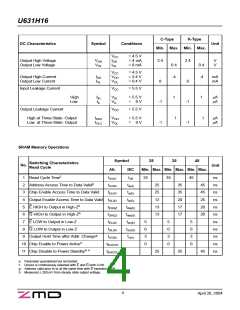
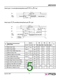
Read Cycle 1: Ai-controlled (during Read cycle: E
G
tcR
(1)
Address Valid
ta(A)
Ai
(2)
DQi
Output Data Valid
Previous Data Valid
Output
tv(A)
(9)
Read Cycle 2: G-, E-controlled (during Read cycle: W = VIH)g
tcR
(1)
Ai
E
Address Valid
(2)
ta(E) (3)
ta(A)
tPD
(5)
(11)
tdis(E)
ten(E) (7)
G
ta(G)
(4)
tdis(G)
(6)
ten(G)
(8)
DQi
High Impedance
Output Data Valid
Output
t
PU (10)
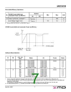
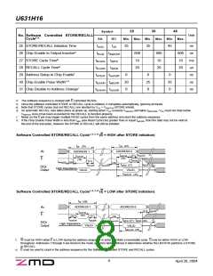
ACTIVE
ICC
STANDBY
Symbol
Alt. #1 Alt. #2
25
35
45
Switching Characteristics
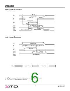
Write Cycle
No.
Unit
IEC
Min. Max. Min. Max. Min. Max.
12 Write Cycle Time
tAVAV
tAVAV
tcW
tw(W)
tsu(W)
tsu(A)
25
20
20
0
35
30
30
0
45
35
35
0
ns
ns
ns
ns
ns
ns
ns
ns
ns
ns
ns
ns
13 Write Pulse Width
tWLWH
14 Write Pulse Width Setup Time
15 Address Setup Time
tWLEH
tAVEL
tAVEH
tAVWL
tAVWH
tELWH
tsu(A-WH)
16 Address Valid to End of Write
17 Chip Enable Setup Time
18 Chip Enable to End of Write
19 Data Setup Time to End of Write
20 Data Hold Time after End of Write
21 Address Hold after End of Write
22 W LOW to Output in High-Zh, i
23 W HIGH to Output in Low-Z
20
20
20
12
0
30
30
30
18
0
35
35
35
20
0
tsu(E)
tw(E)
tsu(D)
th(D)
tELEH
tDVEH
tEHDX
tEHAX
tDVWH
tWHDX
tWHAX
tWLQZ
tWHQX
th(A)
0
0
0
tdis(W)
ten(W)
10
13
15
5
5
5
5
April 20, 2004

 CYPRESS [ CYPRESS ]