CY8C9520A, CY8C9540A
CY8C9560A
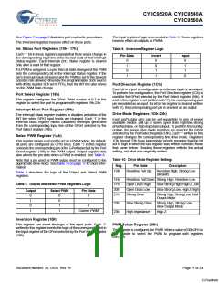
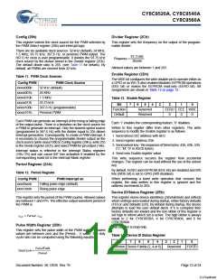
Config (29h)
Divider Register (2Ch)
This register selects the clock source for the PWM selected by
the PWM Select register (28h) and interrupt logic.
This register sets the frequency on the output of the program-
mable divider:
There are six available clock sources: 32 kHz (default), 24 MHz,
1.5 MHz, 93.75 kHz, 367.6 Hz, or previous PWM output. The
367.6 Hz clock is user programmable. It divides the 93.75 kHz
clock source by the divisor stored in the Divider register (2Ch).
The default divide ratio is 255. (see Table 11 for details). By
default, all PWMs are clocked from 32 kHz.
93.75 kHz
Frequency =
.
Divider
Allowed values are between 1 and 255.
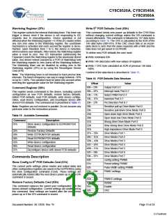
Enable Register (2Dh)
Table 11. PWM Clock Sources
The WDE bit configures the write disable pin to operate either as
a GPIO or as WD. It also enables/disables EEPROM operations
(EEE bit) or makes the EEPROM read-only (EERO bit). Bit
assignments are shown in Table 13 on page 12.
Config PWM
xxxxx000b
xxxxx001b
xxxxx010b
xxxxx011b
xxxxx100b
xxxxx101b
PWM Clock Source
32 kHz (default)
24 MHz
1.5 MHz
Table 13. Enable Register
93.75 kHz
Bit
7
6
5
4
3
2
1
0
367.6 Hz (programmable)
Previous PWM
Function
Default
Reserved
Reserved
EERO EEE WDE
0
0
0
Each PWM can generate an interrupt at the rising or falling edge
of the output pulse. There is a limitation on the clock source for
a PWM to generate an interrupt. Only the slowest speed source
(programmed to 367.6 Hz) with the divider equal to 255 allows
interrupt generation. Consequently, to create a PWM interrupt, it
is necessary to choose the programmable divider output as the
clock source (write xxxxx100b to Config register (29h)), write 255
to the Divide register (2Ch), and select PWM for pin output (1Ah).
Each ’1’ enables the corresponding feature, ’0’ disables.
Writes to this register differ from other registers. The write
sequence to modify the Enable register is as follows:
1. Send device I2C address with bit 0.
2. Send register address 2Dh.
3. Send unlock key - the sequence of three bytes: 43h, 4Dh, 53h;
('C', 'M', 'S' in ASCII bytes).
Interrupt status is reflected in the Interrupt Status registers
(10h-17h) and can cause INT line activation if enabled by the
corresponding mask bit in the Interrupt Mask register:
4. Send new Enable register value.
This write sequence secures the register from accidental
changes. The register can be read without the use of the unlock
key.
Period Register (2Ah)
Table 12. Period Register
By default, EERO and EEPROM (EEE bit) are disabled and WD
line (WDE bit) is set to GPIO (WD disabled).
When performing a burst write operation that crosses this
register, the data written to this register is ignored and the
address increments to 2Eh.
Config PWM
xxxx0xxxb
PWM Interrupt on
Falling pulse edge (default)
Rising pulse edge
xxxx1xxxb
Device ID/Status Register (2Eh)
This register sets the period of the PWM counter. Allowed values
are between 1 and FFh. The effective output waveform period of
the PWM is:
This register stores device identifiers (2xh/4xh/6xh) and reflects
which settings were loaded during startup, either factory defaults
(FD) or user defaults (UD). By default during startup, the device
attempts to load the user default block. If it is corrupted then
factory defaults are loaded and the low nibble of this register is
set high to inform which set is active. The high nibble is always
equal to 2 for CY8C9520A, 4 for CY8C9540A, and 6 for
CY8C9560A.
tOUT = Period ⋅tCLK
Pulse Width Register (2Bh)
This register is read-only.
This register sets the pulse width of the PWM output. Allowed
values are between zero and the (Period - 1) value. The duty
cycle ratio can be computed using the following equation:
Table 14. Device ID Status Register
Bit
7
6
5
4
3
2
1
0
Function Device Family (2, 4,or 6)
Reserved
FD/UD
PulseWidth
DutyCycle =
.
Period
Document Number: 38-12036 Rev. *B
Page 12 of 24
[+] Feedback

 CYPRESS [ CYPRESS ]