CY8C9520A, CY8C9540A
CY8C9560A
Working with PWMs
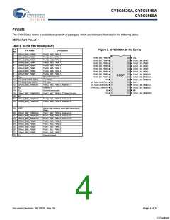
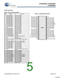
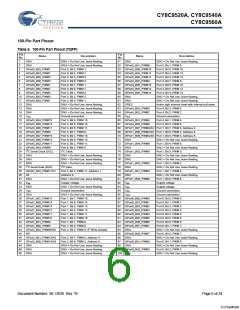
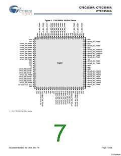
PIN Descriptions
There are four independent PWMs in the CY8C9520A, eight in
the CY8C9540A and sixteen in the CY8C9560A. Each IO pin
can be configured as a PWM output by writing ‘1’ to the corre-
sponding bit of the Select PWM register (see Table 8, “Output
and Select PWM Registers Logic,” on page 11).
Extendable Soft Addressing™
The A0 line defines the corresponding bit of the I2C address.
This pin must be pulled up or down. If A0 is a strong pull up or a
strong pull down (wired through 330 or less resistor to Vdd or
Vss), then that is the only address line being specified and the
A1-A6 lines are used as GPIO. If A0 is a weak pull up or a weak
pull down (connected to Vdd or Vss through 75K- 200K ohm
resistor), then A0 is not the only externally defined address bit.
There is a pin assigned to be A1 if it is needed. This pin can be
pulled up or pulled down strong or weak with a resistor. As with
A0, the type of pull determines whether the address bit is the last
externally defined address bit. Differently from A0, A1 is not
dedicated as an address pin. It is only used if A0 is not the only
address bit externally defined. There are also predefined pins for
A2, A3, A4, A5, and A6 that is only used for addressing if needed.
The last address bit in the chain is pulled strong. That way, only
the number of pins needed to assign the address desired for the
part are allocated as address pins, any pins not used for address
bits can be used as GPIO pins. The Table 2, “Device
Addressing,” on page 3 defines the resulting device I2C address.
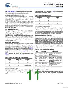
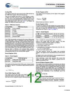
The next step of PWM configuration is clock source selection
using the Config PWM registers. There are six available clock
sources: 32 kHz (default), 24 MHz, 1.5 MHz, 93.75 kHz, 367.6
Hz or previous PWM output. (see Figure 5)
Figure 5. Clock Sources
32 kHz
24mHz
1.5mHz
93.75 kHz
367.6 Hz -
Divider (1-255)
93.75 kHz
Interrupt Pin (INT)
The interrupt output (if enabled) is activated if one of these
events occurs:
By default, 32 kHz is selected as the PWM clock.
■ OneoftheGPIOportpinschangesstateandthecorresponding
bit in the Interrupt Mask register is set low.
PWM Period registers are used to set the output period:
■ When a PWM driven by the slowest clock source (367.6 Hz)
and assigned to a pin changes state and the pin’s corre-
sponding bit in the Interrupt Mask register is set low.
tOUT = Period × tCLK
The interrupt line is deactivated when the master device
performs a read from the corresponding Interrupt Status register.
Allowed values are between 1 and FFh.
The PWM Pulse Width register sets the duration of the PWM
output pulse. Allowed values are between zero and the
(Period-1) value. The duty cycle ratio is computed using thsi
equation:
Write Disable Pin (WD)
If this feature is enabled, ‘0’ allows writes to the EEPROM and
‘1’ blocks any memory writes. This pin is checked immediately
before performing any write to memory. If the EEE bit in the
Enable register is not set (EEPROM disabled) or bit EERO is set
(EEPROM is read-only) then WD line level is ignored.
PulseWidth
DutyCycle = ------------------------------
Period
Note that ‘1’ on this line blocks all commands that perform opera-
tions with EEPROM (see Table 15, “Available Commands,” on
page 13).
This line may be enabled/disabled by bit 1 of the Enable register
(2Dh): ‘1’ enables WD function, ‘0’ disables.
External Reset Pin (XRES)
A full device reset is caused by pulling the XRES pin high. The
XRES pin has an always-on pull down resistor, so it does not
require an external pull down for operation. It can be tied
directly to ground or left open. Behavior after XRES is similar to
POR.
Document Number: 38-12036 Rev. *B
Page 8 of 24
[+] Feedback

 CYPRESS [ CYPRESS ]