CY8C9520A, CY8C9540A
CY8C9560A
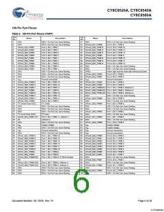
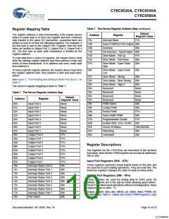
Table 7. The Device Register Address Map (continued)
Register Mapping Table
Default
The register address is auto-incrementing. If the master device
writes or reads data to or from one register and then continues
data transfer in the same I2C transaction, sequential bytes are
written or read to or from the following registers. For example, if
the first byte is sent to the Output Port 1 register, then the next
bytes are written to Output Port 2, Output Port 3, Output Port 4
etc. The first byte of each write transaction is treated as the
register address.
Address
19h
Register
Interrupt Mask
Register Value
FFh
1Ah
1Bh
1Ch
1Dh
1Eh
1Fh
Select PWM for Port Output 00h
Inversion 00h
Pin Direction - Input/Output 00h
Drive Mode - Pull Up
FFh
00h
00h
To read data from a seires of registers, the master device must
write the starting register address byte then perform a start and
series of read transactions. If no address was sent, reads start
from address 0.
Drive Mode - Pull Down
Drive Mode - Open Drain
High
To read a specific register address, the master device must write
the register address byte, then perform a start and read trans-
action.
20h
Drive Mode - Open Drain
Low
00h
21h
22h
23h
24h
25h
26h
27h
28h
29h
2Ah
2Bh
2Ch
2Dh
2Eh
2Fh
30h
Drive Mode - Strong
Drive Mode - Slow Strong
Drive Mode - High-Z
Reserved
00h
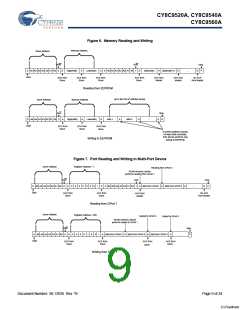
See Figure 7, “Port Reading and Writing in Multi-Port Device,” on
page 9.
00h
00h
The device’s register mapping is listed in Table 7.
None
None
None
None
00h
Reserved
Table 7. The Device Register Address Map
Default
Reserved
Address
Register
Register Value
None
None
None
None
None
None
None
None
FFh
Reserved
00h
Input Port 0
PWM Select
01h
02h
03h
04h
05h
06h
07h
08h
09h
0Ah
0Bh
0Ch
0Dh
0Eh
0Fh
10h
11h
12h
13h
14h
15h
16h
17h
18h
Input Port 1
Config PWM
00h
Input Port 2
Period PWM
FFh
80h
Input Port 3
Pulse Width PWM
Programmable Divider
Input Port 4
FFh
Input Port 5
Enable WDE, EEE, EERO 00h
Input Port 6
Device ID/Status
Watchdog
20h/40h/60h
Input Port 7
00h
00h
Output Port 0
Command
Output Port 1
FFh
Output Port 2
FFh
Register Descriptions
Output Port 3
FFh
Output Port 4
FFh
The registers for the CY8C95xx are described in the sections
that follow. Note that the PWM registers are located at addresses
28h to 2Bh.
Output Port 5
FFh
Output Port 6
FFh
Input Port Registers (00h - 07h)
Output Port 7
FFh
These registers represent actual logical levels on the pins and
are used for IO port reading operations. They are read only. The
Inversion registers changes the state of reads to these ports.
Interrupt Status Port 0
Interrupt Status Port 1
Interrupt Status Port 2
Interrupt Status Port 3
Interrupt Status Port 4
Interrupt Status Port 5
Interrupt Status Port 6
Interrupt Status Port 7
Port Select
00h
00h
00h
Output Port Registers (08h - 0Fh)
00h
These registers are used for writing data to GPIO ports. By
default, all ports are in the pull up mode allowing quasi-bidirec-
tional IO. To allow input operations without reconfiguration, these
registers have to store ’1’s.
00h
00h
00h
Output register data also affects pin states when PWMs are
enabled. See Table 8. Output and Select PWM Registers Logic
for details.
00h
00h
Document Number: 38-12036 Rev. *B
Page 10 of 24
[+] Feedback

 CYPRESS [ CYPRESS ]