PSoC® 3: CY8C32 Family
Data Sheet
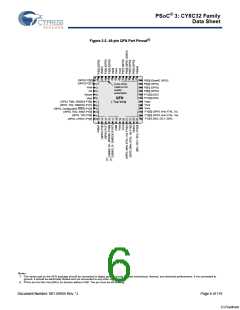
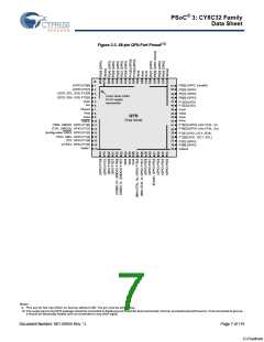
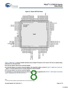
Figure 2-4. 100-pin TQFP Part Pinout
(GPIO) P2[5]
(GPIO) P2[6]
(GPIO) P2[7]
Vddio0
75
1
2
3
4
5
6
74
P0[3] (GPIO,Extref0)
P0[2] (GPIO)
73
72
71
Lines show Vddio
to I/O supply
association
(I2C0: SCL, SIO) P12[4]
(I2C0: SDA, SIO) P12[5]
(GPIO) P6[4]
P0[1] (GPIO)
P0[0] (GPIO)
P4[1] (GPIO)
P4[0] (GPIO)
P12[3] (SIO)
P12[2] (SIO)
Vssd
70
69
(GPIO) P6[5]
(GPIO) P6[6]
(GPIO) P6[7]
7
8
9
68
67
66
65
10
Vssb
Ind
Vboost
Vbat
Vdda
Vssa
11
12
13
14
15
16
17
64
63
Vcca
NC
TQFP
Vssd
XRES
(GPIO) P5[0]
(GPIO) P5[1]
62
61
60
NC
NC
NC
NC
NC
59
58
57
56
55
(GPIO) P5[2]
(GPIO) P5[3]
(TMS, SWDIO, GPIO) P1[0]
18
19
20
21
22
P15[3] (GPIO, kHz XTAL: Xi)
P15[2] (GPIO, kHz XTAL: Xo)
(TCK, SWDCK, GPIO) P1[1]
(configurable XRES, GPIO) P1[2]
(TDO, SWV, GPIO) P1[3]
P12[1] (SIO, I2C1: SDA)
P12[0] (SIO, I2C1: SCL)
P3[7] (GPIO)
54
53
52
51
23
(TDI, GPIO) P1[4]
(nTRST, GPIO) P1[5]
24
25
P3[6] (GPIO)
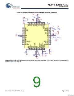
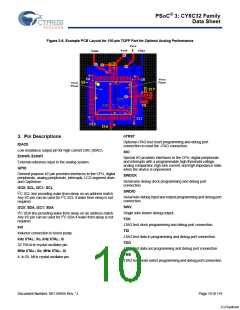
Figure 2-5 and Figure 2-6 show an example schematic and an example PCB layout, for the 100-pin TQFP part, for optimal analog
performance on a two layer board.
The two pins labeled Vddd must be connected together.
The two pins labeled Vccd must be connected together, with capacitance added, as shown in Figure 2-5 and Power System on
page 29. The trace between the two Vccd pins should be as short as possible.
The two pins labeled Vssd must be connected together.
For information on circuit board layout issues for mixed signals, refer to the application note AN57821 - Mixed Signal Circuit Board
Layout Considerations for PSoC® 3 and PSoC 5.
Note
11. Pins are Do Not Use (DNU) on devices without USB. The pin must be left floating.
Document Number: 001-56955 Rev. *J
Page 8 of 119
[+] Feedback

 CYPRESS [ CYPRESS ]