PSoC® 3: CY8C32 Family
Data Sheet
This enables the device to be powered directly from a single
battery or solar cell. In addition, you can use the boost converter
to generate other voltages required by the device, such as a
3.3-V supply for LCD glass drive. The boost’s output is available
on the VBOOST pin, allowing other devices in the application to
be powered from the PSoC.
you can implement a full debugging interface with just three pins.
Using these standard interfaces enables you to debug or
program the PSoC with a variety of hardware solutions from
Cypress or third party vendors. PSoC supports on-chip break
points and 4-KB instruction and data race memory for debug.
Details of the programming, test, and debugging interfaces are
discussed in the “Programming, Debug Interfaces, Resources”
section on page 59 of this datasheet.
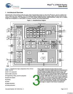
PSoC supports a wide range of low-power modes. These include
a 200-nA hibernate mode with RAM retention and a 1-µA sleep
mode with RTC. In the second mode the optional 32.768-kHz
watch crystal runs continuously and maintains an accurate RTC.
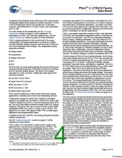
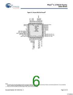
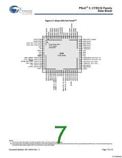
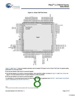
2. Pinouts
Power to all major functional blocks, including the programmable
digital and analog peripherals, can be controlled independently
by firmware. This allows low-power background processing
when some peripherals are not in use. This, in turn, provides a
total device current of only 1.2 mA when the CPU is running at
6 MHz, or 0.8 mA running at 3 MHz.
The Vddio pin that supplies a particular set of pins is indicated
by the black lines drawn on the pinout diagrams in Figure 2-1
through Figure 2-4. Using the Vddio pins, a single PSoC can
support multiple interface voltage levels, eliminating the need for
off-chip level shifters. Each Vddio may sink up to 100 mA total to
its associated I/O pins. On the 68 pin and 100 pin devices each
set of Vddio associated pins may sink up to 100 mA. The 48-pin
device may sink up to 100 mA total for all Vddio0 plus Vddio2
associated I/O pins and 100 mA total for all Vddio1 plus Vddio3
associated I/O pins.
The details of the PSoC power modes are covered in the “Power
System” section on page 29 of this datasheet.
PSoC uses JTAG (4-wire) or SWD (2-wire) interfaces for
programming, debug, and test. The 1-wire SWV may also be
used for “printf” style debugging. By combining SWD and SWV,
Figure 2-1. 48-pin SSOP Part Pinout
(SIO) P12[2]
(SIO) P12[3]
(GPIO) P0[0]
(GPIO) P0[1]
(GPIO) P0[2]
(Extref0, GPIO) P0[3]
Vddio0
Vdda
1
2
48
47
46
45
44
43
42
41
40
39
38
37
36
35
34
33
32
31
30
29
28
27
26
25
Vssa
Lines show
Vddio to I/O
supply
3
Vcca
4
P15[3] (GPIO, kHz XTAL: Xi)
P15[2] (GPIO, kHz XTAL: Xo)
P12[1] (SIO, I2C1: SDA)
P12[0] (SIO, I2C1: SCL)
Vddio3
5
association
6
7
(GPIO) P0[4]
(GPIO) P0[5]
(IDAC0, GPIO) P0[6]
(GPIO) P0[7]
Vccd
8
9
P15[1] (GPIO, MHz XTAL: Xi)
P15[0] (GPIO, MHz XTAL: Xo)
Vccd
10
11
12
13
14
15
16
17
18
19
20
21
22
23
24
Vssd
SSOP
Vssd
Vddd
[6]
Vddd
P15[7] (USBIO, D-, SWDCK)
P15[6] (USBIO, D+, SWDIO)
P1[7] (GPIO)
[6]
(GPIO) P2[3]
(GPIO) P2[4]
Vddio2
P1[6] (GPIO)
(GPIO) P2[5]
(GPIO) P2[6]
(GPIO) P2[7]
Vssb
Vddio1
P1[5] (GPIO, nTRST)
P1[4] (GPIO, TDI)
P1[3] (GPIO, TDO, SWV)
P1[2] (GPIO, configurable XRES)
P1[1] (GPIO, TCK, SWDCK)
P1[0] (GPIO, TMS, SWDIO)
Ind
Vboost
Vbat
Note
6. Pins are Do Not Use (DNU) on devices without USB. The pin must be left floating.
Document Number: 001-56955 Rev. *J
Page 5 of 119
[+] Feedback

 CYPRESS [ CYPRESS ]