PSoC® 3: CY8C32 Family
Data Sheet
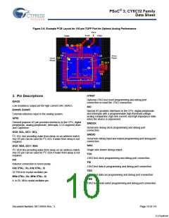
USBIO, D+
4. CPU
Provides D+ connection directly to a USB 2.0 bus. May be used
as a digital I/O pin. Pins are Do Not Use (DNU) on devices
without USB.
4.1 8051 CPU
The CY8C32 devices use a single cycle 8051 CPU, which is fully
compatible with the original MCS-51 instruction set. The
CY8C32 family uses a pipelined RISC architecture, which
executes most instructions in 1 to 2 cycles to provide peak
performance of up to 24 MIPS with an average of 2 cycles per
instruction. The single cycle 8051 CPU runs ten times faster than
a standard 8051 processor.
USBIO, D–
Provides D– connection directly to a USB 2.0 bus. May be used
as a digital I/O pin. Pins are No Connect (NC) on devices without
USB.
Vboost
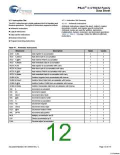
The 8051 CPU subsystem includes these features:
Power sense connection to boost pump.
Single cycle 8051 CPU
Vbat
Up to 64 KB of flash memory, up to 2 KB of EEPROM, and up
to 8 KB of SRAM
Battery supply to boost pump.
Vcca
Programmable nested vector interrupt controller
Direct memory access (DMA) controller
Peripheral HUB (PHUB)
Output of analog core regulator and input to analog core.
Requires a 1-µF capacitor to VSSA. Regulator output not for
external use.
External memory interface (EMIF)
Vccd
Output of digital core regulator and input to digital core. The two
4.2 Addressing Modes
V
CCD pins must be shorted together, with the trace between
The following addressing modes are supported by the 8051:
them as short as possible, and a 1-µF capacitor to VSSD; see
Power System on page 29. Regulator output not for external use.
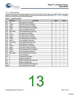
Direct Addressing: The operand is specified by a direct 8-bit
address field. Only the internal RAM and the SFRs can be
accessed using this mode.
Vdda
Supply for all analog peripherals and analog core regulator.
Vdda must be the highest voltage present on the device. All
IndirectAddressing:Theinstructionspecifiestheregisterwhich
contains the address of the operand. The registers R0 or R1
are used to specify the 8-bit address, while the data pointer
(DPTR) register is used to specify the 16-bit address.
other supply pins must be less than or equal to VDDA
.
Vddd
Supply for all digital peripherals and digital core regulator. VDDA
Register Addressing: Certain instructions access one of the
registers (R0 to R7) in the specified register bank. These
instructions are more efficient because there is no need for an
address field.
must be less than or equal to VDDA
.
Vssa
Ground for all analog peripherals.
Register Specific Instructions: Some instructions are specific
to certain registers. For example, some instructions always act
on the accumulator. In this case, there is no need to specify the
operand.
Vssb
Ground connection for boost pump.
Vssd
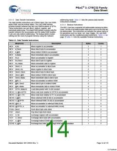
Immediate Constants: Some instructions carry the value of the
constants directly instead of an address.
Ground for all digital logic and I/O pins.
Indexed Addressing: This type of addressing can be used only
for a read of the program memory. This mode uses the data
pointer as the base and the accumulator value as an offset to
read a program memory.
Vddio0, Vddio1, Vddio2, Vddio3
Supply for I/O pins. See pinouts for specific I/O pin to Vddio
mapping. Each Vddio must be tied to a valid operating voltage
(1.71 V to 5.5 V), and must be less than or equal to Vdda. If the
I/O pins associated with Vddio0, Vddio2 or Vddio3 are not used
then that Vddio should be tied to ground (Vssd or Vssa).
Bit Addressing: In this mode, the operand is one of 256 bits.
XRES (and configurable XRES)
External reset pin. Active low with internal pull-up. Pin P1[2] may
be configured to be a XRES pin; see “Nonvolatile Latches
(NVLs)” on page 23.
Document Number: 001-56955 Rev. *J
Page 11 of 119
[+] Feedback

 CYPRESS [ CYPRESS ]