PSoC® 3: CY8C32 Family
Data Sheet
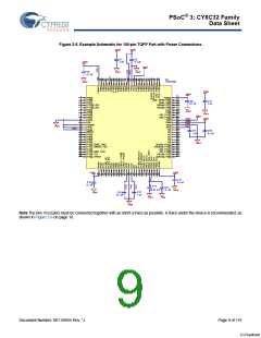
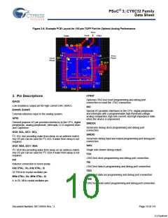
Figure 2-6. Example PCB Layout for 100-pin TQFP Part for Optimal Analog Performance
Vssa
Vssd
Vdda
Vddd
Vssa
Plane
Vssd
Plane
nTRST
3. Pin Descriptions
Optional JTAG test reset programming and debug port
connection to reset the JTAG connection.
IDAC0
Low resistance output pin for high current DAC (IDAC).
SIO
Extref0, Extref1
Special I/O provides interfaces to the CPU, digital peripherals
and interrupts with a programmable high threshold voltage,
analog comparator, high sink current, and high impedance state
when the device is unpowered.
External reference input to the analog system.
GPIO
General purpose I/O pin provides interfaces to the CPU, digital
peripherals, analog peripherals, interrupts, LCD segment drive,
and CapSense.
SWDCK
Serial wire debug clock programming and debug port
connection.
I2C0: SCL, I2C1: SCL
SWDIO
I2C SCL line providing wake from sleep on an address match.
Any I/O pin can be used for I2C SCL if wake from sleep is not
required.
Serial wire debug input and output programming and debug port
connection.
SWV.
I2C0: SDA, I2C1: SDA
I2C SDA line providing wake from sleep on an address match.
Any I/O pin can be used for I2C SDA if wake from sleep is not
required.
Single wire viewer debug output.
TCK
JTAG test clock programming and debug port connection.
Ind
TDI
Inductor connection to boost pump.
kHz XTAL: Xo, kHz XTAL: Xi
32.768-kHz crystal oscillator pin.
MHz XTAL: Xo, MHz XTAL: Xi
4- to 25- MHz crystal oscillator pin.
JTAG test data in programming and debug port connection.
TDO
JTAG test data out programming and debug port connection.
TMS
JTAG test mode select programming and debug port connection.
Document Number: 001-56955 Rev. *J
Page 10 of 119
[+] Feedback

 CYPRESS [ CYPRESS ]