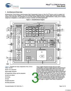
PSoC® 3: CY8C32 Family
Data Sheet
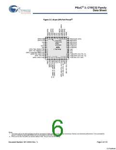
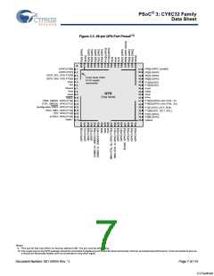
Figure 2-2. 48-pin QFN Part Pinout[8]
(GPIO) P2[6]
(GPIO) P2[7]
36
1
2
P0[3] (Extref0, GPIO)
35 P0[2] (GPIO)
34 P0[1] (GPIO)
33
32
31
Lines show
Vddio to I/O
supply
Vssb
3
4
5
6
Ind
Vboost
P0[0] (GPIO)
P12[3] (SIO)
P12[2] (SIO)
association
Vbat
QFN
( Top View)
(GPIO, TMS, SWDIO) P1[0]
(GPIO, TCK, SWDCK) P1[1]
30 Vdda
29
28
27
7
8
9
10
Vssa
Vcca
(GPIO, Configurable XRES) P1[2]
(GPIO, TDO, SWV) P1[3]
P15[3] (GPIO, kHz XTAL: Xi)
P15[2] (GPIO, kHz XTAL: Xo)
P12[1] (SIO, I2C1: SDA)
(GPIO, TDI) P1[4]
26
25
11
12
(GPIO, nTRST) P1[5]
Notes
7. The center pad on the QFN package should be connected to digital ground (Vssd) for best mechanical, thermal, and electrical performance. If not connected to
ground, it should be electrically floated and not connected to any other signal.
8. PPins are Do Not Use (DNU) on devices without USB. The pin must be left floating.
Document Number: 001-56955 Rev. *J
Page 6 of 119
[+] Feedback

 CYPRESS [ CYPRESS ]