PSoC® 3: CY8C32 Family
Data Sheet
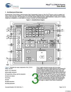
In addition to the flexibility of the UDB array, PSoC also provides
configurable digital blocks targeted at specific functions. For the
CY8C32 family these blocks can include four 16-bit timers,
counters, and PWM blocks; I2C slave, master, and multimaster;
and FS USB.
exchange data without CPU involvement. This allows the CPU
to run slower (saving power) or use those CPU cycles to improve
the performance of firmware algorithms. The single cycle 8051
CPU runs ten times faster than a standard 8051 processor. The
processor speed itself is configurable, allowing you to tune active
power consumption for specific applications.
For more details on the peripherals see the “Example
Peripherals” section on page 41 of this datasheet. For
information on UDBs, DSI, and other digital blocks, see the
“Digital Subsystem” section on page 40 of this datasheet.
PSoC’s nonvolatile subsystem consists of flash, byte-writeable
EEPROM, and nonvolatile configuration options. It provides up
to 64 KB of on-chip flash. The CPU can reprogram individual
blocks of flash, enabling bootloaders. You can enable an ECC
for high reliability applications. A powerful and flexible protection
model secures the user's sensitive information, allowing
selective memory block locking for read and write protection. Up
to 2 KB of byte-writeable EEPROM is available on-chip to store
application data. Additionally, selected configuration options
such as boot speed and pin drive mode are stored in nonvolatile
memory. This allows settings to activate immediately after POR.
PSoC’s analog subsystem is the second half of its unique
configurability. All analog performance is based on a highly
accurate absolute voltage reference with less than 0.9-percent
error over temperature and voltage. The configurable analog
subsystem includes:
Analog muxes
Comparators
Voltage references
ADC
The three types of PSoC I/O are extremely flexible. All I/Os have
many drive modes that are set at POR. PSoC also provides up
to four I/O voltage domains through the VDDIO pins. Every GPIO
has analog I/O, LCD drive[4], CapSense[5], flexible interrupt
generation, slew rate control, and digital I/O capability. The SIOs
on PSoC allow Voh to be set independently of VDDIO when used
as outputs. When SIOs are in input mode they are high
impedance. This is true even when the device is not powered or
when the pin voltage goes above the supply voltage. This makes
the SIO ideally suited for use on an I2C bus where the PSoC may
not be powered when other devices on the bus are. The SIO pins
also have high current sink capability for applications such as
LED drives. The programmable input threshold feature of the
SIO can be used to make the SIO function as a general purpose
analog comparator. For devices with FS USB the USB physical
interface is also provided (USBIO). When not using USB these
pins may also be used for limited digital functionality and device
programming. All of the features of the PSoC I/Os are covered
in detail in the “I/O System and Routing” section on page 34 of
this datasheet.
DAC
All GPIO pins can route analog signals into and out of the device
using the internal analog bus. This allows the device to interface
up to 62 discrete analog signals. The heart of the analog
subsystem is a fast, accurate, configurable delta-sigma ADC
with these features:
Less than 100 µV offset
A gain error of 0.2 percent
INL less than ±1 LSB
DNL less than ±1 LSB
SINAD better than 66 dB
This converter addresses a wide variety of precision analog
applications, including some of the most demanding sensors.
The PSoC device incorporates flexible internal clock generators,
designed for high stability and factory trimmed for high accuracy.
The Internal Main Oscillator (IMO) is the master clock base for
the system, and has 1-percent accuracy at 3 MHz. The IMO can
be configured to run from 3 MHz up to 24 MHz. Multiple clock
derivatives can be generated from the main clock frequency to
meet application needs. The device provides a PLL to generate
system clock frequencies up to 50 MHz from the IMO, external
crystal, or external reference clock. It also contains a separate,
very low-power Internal Low-Speed Oscillator (ILO) for the sleep
and watchdog timers. A 32.768-kHz external watch crystal is
also supported for use in RTC applications. The clocks, together
with programmable clock dividers, provide the flexibility to
integrate most timing requirements.
A high-speed voltage or current DAC supports 8-bit output
signals at an update rate of 8 Msps in current DAC (IDAC) and
1 Msps in voltage DAC (VDAC). It can be routed out of any GPIO
pin. You can create higher resolution voltage PWM DAC outputs
using the UDB array. This can be used to create a pulse width
modulated (PWM) DAC of up to 10 bits, at up to 48 kHz. The
digital DACs in each UDB support PWM, PRS, or delta-sigma
algorithms with programmable widths.
In addition to the ADC and DAC, the analog subsystem provides
multiple comparators.
See the “Analog Subsystem” section on page 51 of this
datasheet for more details.
PSoC’s 8051 CPU subsystem is built around a single cycle
pipelined 8051 8-bit processor running at up to 50 MHz. The
CPU subsystem includes a programmable nested vector
interrupt controller, DMA controller, and RAM. PSoC’s nested
vector interrupt controller provides low latency by allowing the
CPU to vector directly to the first address of the interrupt service
routine, bypassing the jump instruction required by other
architectures. The DMA controller enables peripherals to
The CY8C32 family supports a wide supply operating range from
1.71 V to 5.5 V. This allows operation from regulated supplies
such as 1.8 ± 5 percent, 2.5 V ±10 percent, 3.3 V ± 10 percent,
or 5.0 V ± 10 percent, or directly from a wide range of battery
types. In addition, it provides an integrated high efficiency
synchronous boost converter that can power the device from
supply voltages as low as 0.5 V.
Notes
4. This feature on select devices only. See Ordering Information on page 106 for details.
5. GPIOs with opamp outputs are not recommended for use with CapSense.
Document Number: 001-56955 Rev. *J
Page 4 of 119
[+] Feedback

 CYPRESS [ CYPRESS ]