PSoC® 3: CY8C32 Family
Data Sheet
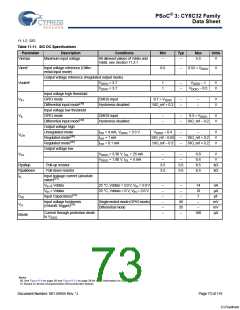
Table 11-14. USBIO AC Specifications
Parameter
Description
Conditions
Min
Typ
Max
Units
Tdrate
Full-speed data rate average bit rate
12 – 0.25%
12
12 +
0.25%
MHz
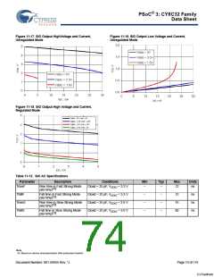
Tjr1
Tjr2
Tdj1
Receiver data jitter tolerance to next
transition
Receiver data jitter tolerance to pair
transition
Driver differential jitter to next
transition
–8
–5
–
–
–
8
ns
ns
ns
5
–3.5
3.5
Tdj2
Tfdeop
Driver differential jitter to pair transition
Source jitter fordifferentialtransitionto
SE0 transition
–4
–2
–
–
4
5
ns
ns
Tfeopt
Tfeopr
Tfst
Source SE0 interval of EOP
Receiver SE0 interval of EOP
Width of SE0 interval during differ-
ential transition
160
82
–
–
–
–
175
–
14
ns
ns
ns
Fgpio_out GPIO mode output operating
frequency
3 V ≤ VDDD ≤ 5.5 V
DDD = 1.71 V
VDDD > 3 V, 25 pF load
DDD = 1.71 V, 25 pF load
–
–
–
–
–
–
–
–
–
–
–
–
20
6
12
40
12
40
MHz
MHz
ns
ns
ns
V
Tr_gpio
Rise time, GPIO mode, 10%/90%
VDDD
V
Tf_gpio
Fall time, GPIO mode, 90%/10% VDDD VDDD > 3 V, 25 pF load
DDD = 1.71 V, 25 pF load
V
ns
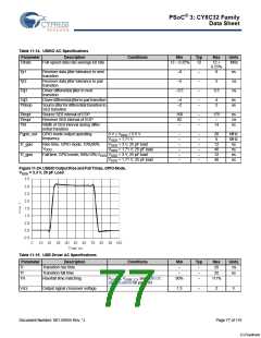
Figure11-24. USBIOOutputRiseandFallTimes, GPIOMode,
VDDD = 3.3 V, 25 pF Load
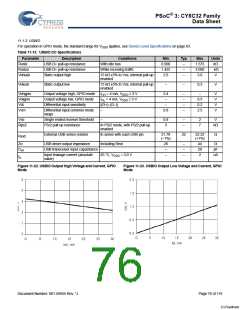
Table 11-15. USB Driver AC Specifications
Parameter
Tr
Description
Transition rise time
Conditions
Min
–
Typ
–
Max
20
Units
ns
Tf
Transition fall time
–
–
20
ns
TR
Rise/fall time matching
VUSB_5, VUSB_3.3, see USB DC
Specifications on page 93
90%
–
111%
Vcrs
Output signal crossover voltage
1.3
–
2
V
Document Number: 001-56955 Rev. *J
Page 77 of 119
[+] Feedback

 CYPRESS [ CYPRESS ]