PSoC® 3: CY8C32 Family
Data Sheet
11.2.2 Voltage Reference
Table 11-21. Voltage Reference Specifications
See also ADC external reference specifications in Section 11.2.1.
Parameter
Description
Precision reference voltage
Conditions
Min
Typ
Max
Units
VREF
Initial trim
1.014 (–1%) 1.024 1.034 (+1%)
V
11.2.3 Analog Globals
Table 11-22. Analog Globals Specifications
Parameter
Description
Resistance pin-to-pin through analog global[37]
Conditions
VDDA = 3.0 V
VDDA = 3.0 V
Min
–
Typ
939
721
Max
1461
1135
Units
Ω
Rppag
Rppmuxbus Resistance pin-to-pin through analog mux bus[37]
–
Ω
11.2.4 Comparator
Table 11-23. Comparator DC Specifications
Parameter
Description
Conditions
Min
Typ
Max
Units
Input offset voltage in fast mode
Factory trim, Vdda > 2.7 V,
Vin ≥ 0.5 V
–
10
mV
VOS
Input offset voltage in slow mode
Input offset voltage in fast mode[38]
Input offset voltage in slow mode[38]
Factory trim, Vin ≥ 0.5 V
Custom trim
–
–
–
–
9
4
4
–
mV
mV
mV
mV
–
–
VOS
VOS
Custom trim
Input offset voltage in ultra low-power
mode
±12
VHYST
VICM
Hysteresis
Hysteresis enable mode
High current / fast mode
Low current / slow mode
Ultra low power mode
–
VSSA
VSSA
VSSA
–
10
–
32
VDDA – 0.1
VDDA
VDDA – 0.9
–
mV
V
Input common mode voltage
–
V
–
CMRR
ICMP
Common mode rejection ratio
High current mode/fast mode[39]
Low current mode/slow mode[39]
Ultra low-power mode[39]
50
–
dB
µA
µA
µA
–
400
–
–
100
–
6
–
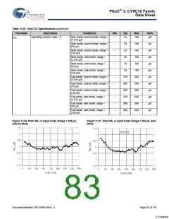
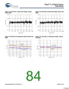
Table 11-24. Comparator AC Specifications
Parameter
Description
Conditions
Min
Typ
Max
110
200
–
Units
ns
Response time, high current mode[39]
Response time, low current mode[39]
Response time, ultra low-power mode[39] 50 mV overdrive, measured pin-to-pin
50 mV overdrive, measured pin-to-pin
–
–
–
75
155
55
Tresp
50 mV overdrive, measured pin-to-pin
ns
µs
Notes
37. The resistance of the analog global and analog mux bus is high if VDDA ≤ 2.7 V, and the chip is in either sleep or hibernate mode. Use of analog global and analog
mux bus under these conditions is not recommended
38. The recommended procedure for using a custom trim value for the on-chip comparators can be found in the TRM.
39. Based on device characterization (Not production tested).
Document Number: 001-56955 Rev. *J
Page 81 of 119
[+] Feedback

 CYPRESS [ CYPRESS ]