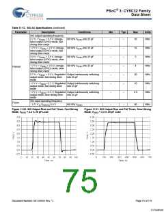
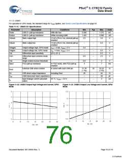
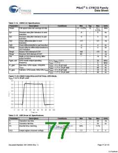
PSoC® 3: CY8C32 Family
Data Sheet
11.2 Analog Peripherals
Specifications are valid for –40 °C ≤ TA ≤ 85 °C and TJ ≤ 100 °C, except where noted. Specifications are valid for 1.71 V to 5.5 V,
except where noted.
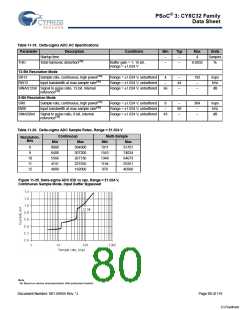
11.2.1 Delta-sigma ADC
Unless otherwise specified, operating conditions are:
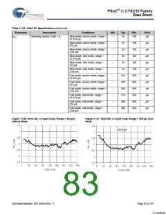
Operation in continuous sample mode
fclk = 6.144 MHz
Reference = 1.024 V internal reference bypassed on P3.2 or P0.3
Unless otherwise specified, all charts and graphs show typical values
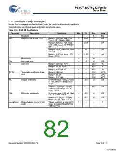
Table 11-18. 12-bit Delta-sigma ADC DC Specifications
Parameter
Description
Conditions
Min
Typ
Max
Units
Resolution
8
–
12
bits
No. of
GPIO
Number of channels, single ended
–
–
–
Differential pair is formed using a
pair of GPIOs.
Yes
Buffered, buffer gain = 1, Range =
±1.024 V, 25 °C
No. of
GPIO/2
Number of channels, differential
Monotonic
–
–
–
–
–
–
–
–
–
Ge
Gain error
±0.2
%
Buffered, buffer gain = 1, Range =
±1.024 V
Buffered, 16-bit mode, VDDA = 2.7 V,
25 °C
Buffer gain = 1, 16-bit,
Range = ±1.024 V
Gd
Gain drift
–
–
–
–
50
ppm/°C
mV
Vos
TCVos
Input offset voltage
±0.1
Temperature coefficient, input offset
voltage
Input voltage range, single ended[34]
Input voltage range, differential unbuf-
fered[34]
–
–
–
–
55
µV/°C
VSSA
VSSA
VDDA
VDDA
V
V
Input voltage range, differential,
VSSA
–
VDDA – 1
V
buffered[34]
INL12
DNL12
INL8
DNL8
Rin_Buff
Integral non linearity[34]
Differential non linearity[34]
Integral non linearity[34]
Differential non linearity[34]
ADC input resistance
Range = ±1.024 V, unbuffered
Range = ±1.024 V, unbuffered
Range = ±1.024 V, unbuffered
Range = ±1.024 V, unbuffered
Input buffer used
–
–
–
–
10
–
–
–
–
–
±1
±1
±1
±1
–
LSB
LSB
LSB
LSB
MΩ
Input buffer bypassed, 12 bit,
Range = ±1.024 V
Rin_ADC12 ADC input resistance
–
148[35]
–
kΩ
ADC external reference input voltage, see
also internal reference in Voltage
Reference on page 81
Vextref
Pins P0[3], P3[2]
0.9
–
1.3
V
Current Consumption
IDD_12
Current consumption, 12 bit[34]
IBUFF
Buffer current consumption[34]
192 ksps, unbuffered
–
–
–
–
1.4
2.5
mA
mA
Notes
34. Based on device characterization (Not production tested).
35. By using switched capacitors at the ADC input an effective input resistance is created. Holding the gain and number of bits constant, the resistance is proportional
to the inverse of the clock frequency. This value is calculated, not measured. For more information see the Technical Reference Manual.
Document Number: 001-56955 Rev. *J
Page 79 of 119
[+] Feedback

 CYPRESS [ CYPRESS ]