PSoC® 3: CY8C32 Family
Data Sheet
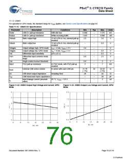
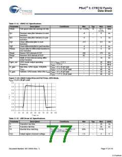
11.1.2 SIO
Table 11-11. SIO DC Specifications
Parameter
Vinmax
Description
Conditions
Min
Typ
Max
Units
Maximum input voltage
All allowed values of Vddio and
Vddd, see Section 11.2.1
–
–
5.5
V
Vinref
Input voltage reference (Differ-
ential input mode)
0.5
–
0.52 × VDDIO
V
Output voltage reference (Regulated output mode)
VDDIO > 3.7
Voutref
1
1
–
–
VDDIO – 1
V
V
VDDIO < 3.7
VDDIO – 0.5
Input voltage high threshold
VIH
GPIO mode
CMOS input
0.7 × VDDIO
–
–
–
–
V
V
Differential input mode[30]
Input voltage low threshold
GPIO mode
Differential input mode[30]
Output voltage high
Unregulated mode
Regulated mode[30]
Regulated mode[30]
Output voltage low
Hysteresis disabled
SIO_ref + 0.2
VIL
CMOS input
–
–
–
–
0.3 × VDDIO
V
V
Hysteresis disabled
SIO_ref – 0.2
I
OH = 4 mA, VDDIO = 3.3 V
VDDIO – 0.4
SIO_ref – 0.65
SIO_ref – 0.3
–
–
–
–
V
V
V
VOH
IOH = 1 mA
SIO_ref + 0.2
SIO_ref + 0.2
IOH = 0.1 mA
VOL
VDDIO = 3.30 V, IOL = 25 mA
–
–
0.8
0.4
8.5
8.5
V
V
VDDIO = 1.80 V, IOL = 4 mA
–
–
Rpullup
Rpulldown
IIL
Pull-up resistor
3.5
3.5
5.6
5.6
kΩ
kΩ
Pull-down resistor
Input leakage current (absolute
value)[31]
VIH < Vddsio
25 °C, Vddsio = 3.0 V, VIH = 3.0 V
25 °C, Vddsio = 0 V, VIH = 3.0 V
–
–
–
–
–
–
–
–
14
10
7
nA
µA
pF
VIH > Vddsio
CIN
VH
Input Capacitance[31]
–
Input voltage hysteresis
(Schmitt-Trigger)[31]
Single ended mode (GPIO mode)
Differential mode
40
35
–
–
mV
mV
µA
–
Current through protection diode
to VSSIO
100
Idiode
Notes
30. See Figure 6-9 on page 36 and Figure 6-12 on page 39 for more information on SIO reference
31. Based on device characterization (Not production tested).
Document Number: 001-56955 Rev. *J
Page 73 of 119
[+] Feedback

 CYPRESS [ CYPRESS ]