PSoC® 3: CY8C32 Family
Data Sheet
1. Architectural Overview
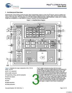
Introducing the CY8C32 family of ultra low-power, flash Programmable System-on-Chip (PSoC®) devices, part of a scalable 8-bit
PSoC 3 and 32-bit PSoC 5 platform. The CY8C32 family provides configurable blocks of analog, digital, and interconnect circuitry
around a CPU subsystem. The combination of a CPU with a flexible analog subsystem, digital subsystem, routing, and I/O enables
a high level of integration in a wide variety of consumer, industrial, and medical applications.
Figure 1-1. Simplified Block Diagram
Analog Interconnect
Digital Interconnect
Digital System
System Wide
Resources
I2C
Master/
Slave
Universal Digital Block Array (24x UDB)
8- Bit
Timer
Quadrature Decoder
16- Bit PRS
16- Bit
PWM
4- 33 MHz
( Optional)
UDB
UDB
UDB
UDB
UDB
UDB
UDB
UDB
UDB
UDB
UDB
UDB
22 Ω
Xtal
Osc
USB
PHY
UDB
FS USB
2.0
UDB
UDB
UDB
I2C Slave
UDB
8- Bit
Timer
4x
8- Bit SPI
Logic
Timer
Counter
PWM
12- Bit SPI
UDB
UDB
UDB
UDB
IMO
Logic
32.768 KHz
( Optional)
UDB
UDB
UDB
UART
12- Bit PWM
RTC
Timer
System Bus
Program
Debug
Memory System
CPU System
&
WDT
and
Wake
8051 or
Interrupt
EEPROM
SRAM
Cortex M3
CPU
Program
Controller
Debug &
Trace
PHUB
DMA
FLASH
EMIF
Boundary
Scan
ILO
Clocking System
Analog System
ADC
Power Management
System
LCD Direct
Drive
POR and
LVD
Sleep
Power
Del Sig
ADC
+
Temperature
Sensor
2 x
CMP
1.8V LDO
SMP
DAC
-
CapSense
0. 5 to5.5V
( Optional)
Figure 1-1 illustrates the major components of the CY8C32
family. They are:
PSoC’s digital subsystem provides half of its unique
configurability. It connects a digital signal from any peripheral to
any pin through the Digital System Interconnect (DSI). It also
provides functional flexibility through an array of small, fast,
low-power UDBs. PSoC Creator provides a library of prebuilt and
tested standard digital peripherals (UART, SPI, LIN, PRS, CRC,
timer, counter, PWM, AND, OR, and so on) that are mapped to
the UDB array. You can also easily create a digital circuit using
boolean primitives by means of graphical design entry. Each
UDB contains programmable array logic (PAL)/programmable
logic device (PLD) functionality, together with a small state
machine engine to support a wide variety of peripherals.
8051 CPU subsystem
Nonvolatile subsystem
Programming, debug, and test subsystem
Inputs and outputs
Clocking
Power
Digital subsystem
Analog subsystem
Document Number: 001-56955 Rev. *J
Page 3 of 119
[+] Feedback

 CYPRESS [ CYPRESS ]