PSoC® 3: CY8C32 Family
Data Sheet
6.4.15 Over Voltage Tolerance
Analog
High current IDAC output
External reference inputs
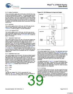
All I/O pins provide an over voltage tolerance feature at any
operating VDD
.
There are no current limitations for the SIO pins as they present a
6.4.19 JTAG Boundary Scan
high impedance load to the external circuit where VDDIO < VIN
5.5 V.
<
The device supports standard JTAG boundary scan chains on all
I/O pins for board level test.
TheGPIOpinsmustbelimitedto100µAusingacurrentlimiting
resistor. GPIO pins clamp the pin voltage to approximately one
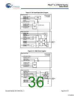
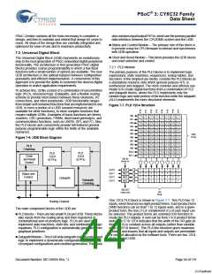
7. Digital Subsystem
diode above the VDDIO supply where VDDIO < VIN < VDDA
.
The digital programmable system creates application specific
combinations of both standard and advanced digital peripherals
and custom logic functions. These peripherals and logic are then
interconnected to each other and to any pin on the device,
providing a high level of design flexibility and IP security.
In case of a GPIO pin configured for analog input/output, the
analog voltage on the pin must not exceed the VDDIO supply
voltage to which the GPIO belongs.
A common application for this feature is connection to a bus such
as I2C where different devices are running from different supply
voltages. In the I2C case, the PSoC chip is configured into the
Open Drain, Drives Low mode for the SIO pin. This allows an
external pull-up to pull the I2C bus voltage above the PSoC pin
supply. For example, the PSoC chip could operate at 1.8 V, and
an external device could run from 5 V. Note that the SIO pin’s VIH
and VIL levels are determined by the associated VDDIO supply
pin.
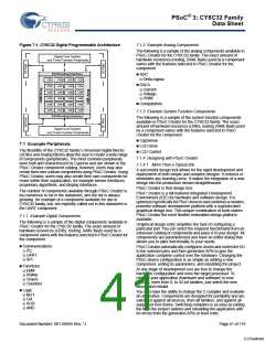
The features of the digital programmable system are outlined
here to provide an overview of capabilities and architecture. You
do not need to interact directly with the programmable digital
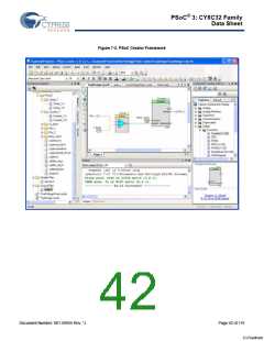
system at the hardware and register level. PSoC Creator
provides a high level schematic capture graphical interface to
automatically place and route resources similar to PLDs.
The main components of the digital programmable system are:
Universal Digital Blocks (UDB) – These form the core
functionality of the digital programmable system. UDBs are a
collection of uncommitted logic (PLD) and structural logic
(Datapath) optimized to create all common embedded
peripherals and customized functionality that are application or
design specific.
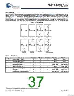
The I/O pin must be configured into a high impedance drive
mode, open drain low drive mode, or pull-down drive mode, for
over voltage tolerance to work properly. Absolute maximum
ratings for the device must be observed for all I/O pins.
6.4.16 Reset Configuration
While reset is active all I/Os are reset to and held in the High
Impedance Analog state. After reset is released, the state can be
reprogrammed on a port-by-port basis to pull-down or pull-up. To
ensure correct reset operation, the port reset configuration data
is stored in special nonvolatile registers. The stored reset data is
automatically transferred to the port reset configuration registers
at reset release.
Universal Digital Block Array – UDB blocks are arrayed within
a matrix of programmable interconnect. The UDB array
structure is homogeneous and allows for flexible mapping of
digital functions onto the array. The array supports extensive
and flexible routing interconnects between UDBs and the
Digital System Interconnect.
Digital System Interconnect (DSI) – Digital signals from
Universal Digital Blocks (UDBs), fixed function peripherals, I/O
pins, interrupts, DMA, and other system core signals are
attached to the Digital System Interconnect to implement full
featureddeviceconnectivity.TheDSIallowsanydigitalfunction
to any pin or other feature routability when used with the
Universal Digital Block Array.
6.4.17 Low-Power Functionality
In all low-power modes the I/O pins retain their state until the part
is awakened and changed or reset. To awaken the part, use a
pin interrupt, because the port interrupt logic continues to
function in all low-power modes.
6.4.18 Special Pin Functionality
Some pins on the device include additional special functionality
in addition to their GPIO or SIO functionality. The specific special
function pins are listed in Pinouts on page 5. The special features
are:
Digital
4- to 25- MHz crystal oscillator
32.768-kHz crystal oscillator
Wake from sleep on I2C address match. Any pin can be used
for I2C if wake from sleep is not required.
JTAG interface pins
SWD interface pins
SWV interface pins
External reset
Document Number: 001-56955 Rev. *J
Page 40 of 119
[+] Feedback

 CYPRESS [ CYPRESS ]