PSoC® 3: CY8C32 Family
Data Sheet
dividers. This is only possible if there are multiple precision clock
sources.
Each clock divider consists of an 8-input multiplexer, a 16-bit
clock divider (divide by 2 and higher) that generates ~50 percent
duty cycle clocks, system clock resynchronization logic, and
deglitch logic. The outputs from each digital clock tree can be
routed into the digital system interconnect and then brought back
into the clock system as an input, allowing clock chaining of up
to 32 bits.
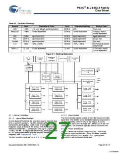
6.1.3 Clock Distribution
All seven clock sources are inputs to the central clock distribution
system. The distribution system is designed to create multiple
high precision clocks. These clocks are customized for the
design’s requirements and eliminate the common problems
found with limited resolution prescalers attached to peripherals.
The clock distribution system generates several types of clock
trees.
6.1.4 USB Clock Domain
The USB clock domain is unique in that it operates largely
asynchronously from the main clock network. The USB logic
contains a synchronous bus interface to the chip, while running
on an asynchronous clock to process USB data. The USB logic
requires a 48 MHz frequency. This frequency can be generated
from different sources, including DSI clock at 48 MHz or doubled
value of 24 MHz from internal oscillator, DSI signal, or crystal
oscillator.
The system clock is used to select and supply the fastest clock
in the system for general system clock requirements and clock
synchronization of the PSoC device.
Bus Clock 16-bit divider uses the system clock to generate the
system's bus clock used for data transfers. Bus clock is the
source clock for the CPU clock divider.
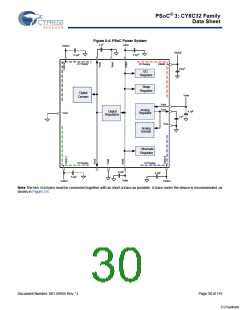
6.2 Power System
Eight fully programmable 16-bit clock dividers generate digital
system clocks for general use in the digital system, as
configured by the design’s requirements. Digital system clocks
can generate custom clocks derived from any of the seven
clock sources for any purpose. Examples include baud rate
generators, accurate PWM periods, and timer clocks, and
many others. If more than eight digital clock dividers are
required, theUniversalDigitalBlocks(UDBs)andfixedfunction
Timer/Counter/PWMs can also generate clocks.
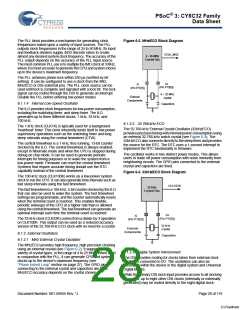
The power system consists of separate analog, digital, and I/O
supply pins, labeled Vdda, Vddd, and Vddiox, respectively. It
also includes two internal 1.8 V regulators that provide the digital
(Vccd) and analog (Vcca) supplies for the internal core logic. The
output pins of the regulators (Vccd and Vcca) and the Vddio pins
must have capacitors connected as shown in Figure 6-4. The
two Vccd pins must be shorted together, with as short a trace as
possible, and connected to a 1-µF ±10-percent X5R capacitor.
The power system also contains a sleep regulator, an I2C
regulator, and a hibernate regulator.
Four16-bitclockdividersgenerateclocksfortheanalogsystem
components that require clocking, such as ADC. The analog
clockdividersincludeskewcontroltoensurethatcriticalanalog
events do not occur simultaneously with digital switching
events. This is done to reduce analog system noise.
Document Number: 001-56955 Rev. *J
Page 29 of 119
[+] Feedback

 CYPRESS [ CYPRESS ]