PSoC® 3: CY8C32 Family
Data Sheet
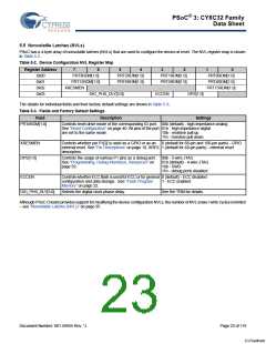
5.5 Nonvolatile Latches (NVLs)
PSoC has a 4-byte array of nonvolatile latches (NVLs) that are used to configure the device at reset. The NVL register map is shown
in Table 5-2.
Table 5-2. Device Configuration NVL Register Map
Register Address
7
6
5
4
3
2
1
0
0x00
0x01
0x02
0x03
PRT3RDM[1:0]
PRT12RDM[1:0]
PRT2RDM[1:0]
PRT6RDM[1:0]
PRT1RDM[1:0]
PRT5RDM[1:0]
PRT0RDM[1:0]
PRT4RDM[1:0]
PRT15RDM[1:0]
XRESMEN
DIG_PHS_DLY[3:0]
ECCEN
DPS[1:0]
The details for individual fields and their factory default settings are shown in Table 5-3:.
Table 5-3. Fields and Factory Default Settings
Field
Description
Settings
PRTxRDM[1:0]
Controls reset drive mode of the corresponding IO port. 00b (default) - high impedance analog
See “Reset Configuration” on page 40. All pins of the port 01b - high impedance digital
are set to the same mode.
10b - resistive pull up
11b - resistive pull down
XRESMEN
DPS{1:0]
Controls whether pin P1[2] is used as a GPIO or as an
external reset. See “Pin Descriptions” on page 10, XRES 1 (default for 48-pin parts) - external reset
description.
0 (default for 68-pin and 100-pin parts) - GPIO
Controls the usage of various P1 pins as a debug port. 00b - 5-wire JTAG
See “Programming, Debug Interfaces, Resources” on
page 59.
01b (default) - 4-wire JTAG
10b - SWD
11b - debug ports disabled
ECCEN
Controls whether ECC flash is used for ECC or for general 0 (default) - ECC disabled
configuration and data storage. See “Flash Program
1 - ECC enabled
Memory” on page 22.
DIG_PHS_DLY[3:0]
Selects the digital clock phase delay.
See the TRM for details.
Although PSoC Creator provides support for modifying the device configuration NVLs, the number of NVL erase / write cycles is limited
– see “Nonvolatile Latches (NVL))” on page 95.
Document Number: 001-56955 Rev. *J
Page 23 of 119
[+] Feedback

 CYPRESS [ CYPRESS ]