PSoC® 3: CY8C32 Family
Data Sheet
I/O Port SFRs
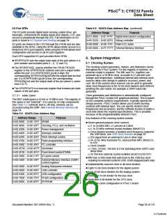
Table 5-5. XDATA Data Address Map (continued)
Address Range Purpose
The I/O ports provide digital input sensing, output drive, pin
interrupts, connectivity for analog inputs and outputs, LCD, and
access to peripherals through the DSI. Full information on I/O
ports is found in I/O System and Routing on page 34.
0×01 0000 – 0×01 FFFF Digital Interconnect configuration
0×05 0220 – 0×05 02F0 Debug controller
I/O ports are linked to the CPU through the PHUB and are also
available in the SFRs. Using the SFRs allows faster access to a
limited set of I/O port registers, while using the PHUB allows boot
configuration and access to all I/O port registers.
0×08 0000 – 0×08 1FFF Flash ECC bytes
0×80 0000 – 0×FF FFFF External Memory Interface
Each SFR supported I/O port provides three SFRs:
6. System Integration
SFRPRTxDR sets the output data state of the port (where x is
port number and includes ports 0 – 6, 12 and 15).
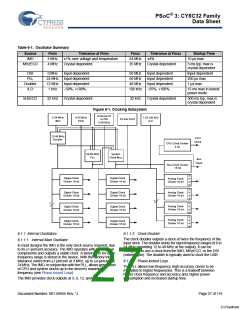
6.1 Clocking System
The clocking system generates, divides, and distributes clocks
throughout the PSoC system. For the majority of systems, no
external crystal is required. The IMO and PLL together can
generate up to a 50 MHz clock, accurate to ±1 percent over
voltage and temperature. Additional internal and external clock
sources allow each design to optimize accuracy, power, and
cost. All of the system clock sources can be used to generate
other clock frequencies in the 16-bit clock dividers and UDBs for
anything the user wants, for example a UART baud rate
generator.
The SFRPRTxSEL selects whether the PHUB PRTxDR
register or the SFRPRTxDR controls each pin’s output buffer
within the port. If a SFRPRTxSEL[y] bit is high, the
corresponding SFRPRTxDR[y] bit sets the output state for that
pin. If a SFRPRTxSEL[y] bit is low, the corresponding
PRTxDR[y] bit sets the output state of the pin (where y varies
from 0 to 7).
The SFRPRTxPS is a read only register that contains pin state
values of the port pins.
Clock generation and distribution is automatically configured
through the PSoC Creator IDE graphical interface. This is based
on the complete system’s requirements. It greatly speeds the
design process. PSoC Creator allows you to build clocking
systems with minimal input. You can specify desired clock
frequencies and accuracies, and the software locates or builds a
clock that meets the required specifications. This is possible
because of the programmability inherent PSoC.
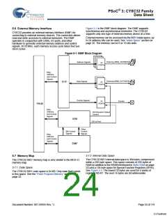
5.7.3.1 xdata Space
The 8051 xdata space is 24-bit, or 16 MB in size. The majority of
this space is not “external”—it is used by on-chip components.
See Table 5-5. External, that is, off-chip, memory can be
accessed using the EMIF. See External Memory Interface on
page 24.
Table 5-5. XDATA Data Address Map
Address Range
Purpose
Key features of the clocking system include:
0×00 0000 – 0×00 1FFF SRAM
Seven general purpose clock sources
0×00 4000 – 0×00 42FF Clocking, PLLs, and oscillators
0×00 4300 – 0×00 43FF Power management
0×00 4400 – 0×00 44FF Interrupt controller
0×00 4500 – 0×00 45FF Ports interrupt control
0×00 4700 – 0×00 47FF Flash programming interface
0×00 4900 – 0×00 49FF I2C controller
3- to 24-MHz IMO, ±1 percent at 3 MHz
4- to 25-MHz external crystal oscillator (MHzECO)
Clock doubler provides a doubled clock frequency output for
the USB block, see USB Clock Domain on page 29
DSI signal from an external I/O pin or other logic
24- to 50- MHz fractional PLL sourced from IMO, MHzECO,
or DSI
Clock Doubler
0×00 4E00 – 0×00 4EFF Decimator
1-kHz, 33-kHz, 100-kHz ILO for watchdog timer (WDT) and
sleep timer
0×00 4F00 – 0×00 4FFF Fixed timer/counter/PWMs
0×00 5000 – 0×00 51FF I/O ports control
32.768-kHz external crystal oscillator (kHzECO) for RTC
IMO has a USB mode that auto locks to the USB bus clock
requiring no external crystal for USB. (USB equipped parts only)
0×00 5400 – 0×00 54FF External Memory Interface (EMIF)
control registers
Independently sourced clock in all clock dividers
Eight 16-bit clock dividers for the digital system
Four 16-bit clock dividers for the analog system
Dedicated 16-bit divider for the bus clock
Dedicated 4-bit divider for the CPU clock
0×00 5800 – 0×00 5FFF Analog Subsystem interface
0×00 6000 – 0×00 60FF USB controller
0×00 6400 – 0×00 6FFF UDB configuration
0×00 7000 – 0×00 7FFF PHUB configuration
0×00 8000 – 0×00 8FFF EEPROM
Automatic clock configuration in PSoC Creator
Document Number: 001-56955 Rev. *J
Page 26 of 119
[+] Feedback

 CYPRESS [ CYPRESS ]