PSoC® 3: CY8C32 Family
Data Sheet
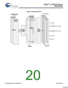
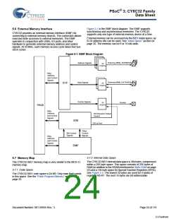
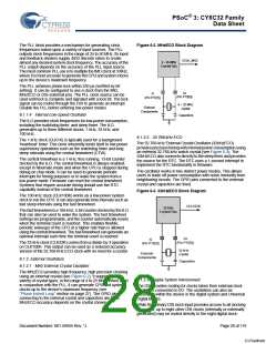
Figure 5-1 is the EMIF block diagram. The EMIF supports
synchronous and asynchronous memories. The CY8C32
supports only one type of external memory device at a time.
5.6 External Memory Interface
CY8C32 provides an external memory interface (EMIF) for
connecting to external memory devices. The connection allows
read and write accesses to external memories. The EMIF
operates in conjunction with UDBs, I/O ports, and other
hardware to generate external memory address and control
signals. At 33 MHz, each memory access cycle takes four bus
clock cycles.
External memory can be accessed via the 8051 xdata space; up
to 24 address bits can be used. See “xdata Space” section on
page 26. The memory can be 8 or 16 bits wide.
Figure 5-1. EMIF Block Diagram
External_MEM_ ADDR[23:0]
External_MEM_DATA[15:0]
Address Signals
IO
PORTs
Data,
Address,
and Control
Signals
Data Signals
IO IF
IO
PORTs
Control Signals
Control
IO
PORTs
PHUB
Data,
Address,
and Control
Signals
DSI Dynamic Output
Control
UDB
DSI to Port
Other
EM Control
Signals
Control
Signals
Data,
Address,
and Control
Signals
EMIF
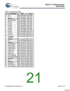
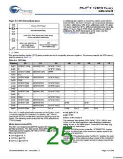
5.7.2 Internal Data Space
5.7 Memory Map
The CY8C32 8051 internal data space is 384 bytes, compressed
within a 256-byte space. This space consists of 256 bytes of
RAM (in addition to the SRAM mentioned in Static RAM on page
22) and a 128-byte space for Special Function Registers (SFRs).
See Figure 5-2. The lowest 32 bytes are used for 4 banks of
registers R0-R7. The next 16 bytes are bit-addressable.
The CY8C32 8051 memory map is very similar to the MCS-51
memory map.
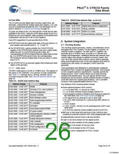
5.7.1 Code Space
The CY8C32 8051 code space is 64 KB. Only main flash exists
in this space. See the “Flash Program Memory” section on
page 22.
Document Number: 001-56955 Rev. *J
Page 24 of 119
[+] Feedback

 CYPRESS [ CYPRESS ]