PSoC® 3: CY8C32 Family
Data Sheet
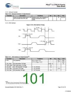
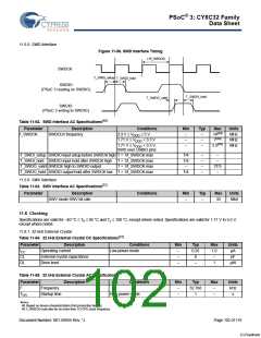
11.5.5 SWD Interface
Figure 11-56. SWD Interface Timing
(1/f_SWDCK)
SWDCK
SWDIO
T_SWDI_setup
T_SWDI_hold
(PSoC 3 reading on SWDIO)
T_SWDO_hold
T_SWDO_valid
SWDIO
(PSoC 3 writing to SWDIO)
Table 11-62. SWD Interface AC Specifications[48]
Parameter
Description
SWDCLK frequency
Conditions
Min
–
Typ
–
Max
14[49]
7[49]
Units
MHz
MHz
MHz
f_SWDCK
3.3 V ≤ VDDD ≤ 5 V
1.71 V ≤ VDDD < 3.3 V
1.71 V ≤ VDDD < 3.3 V,
SWD over USBIO pins
–
–
–
–
5.5[49]
T_SWDI_setup SWDIO input setup before SWDCK high T = 1/f_SWDCK max
T/4
T/4
–
–
–
–
–
–
–
T_SWDI_hold SWDIO input hold after SWDCK high
T_SWDO_valid SWDCK high to SWDIO output
T = 1/f_SWDCK max
T = 1/f_SWDCK max
2T/5
–
T_SWDO_hold SWDIO output hold after SWDCK low T = 1/f_SWDCK max
T/4
11.5.6 SWV Interface
[22]
Table 11-63. SWV Interface AC Specifications
Parameter
Description
Conditions
Min
Typ
Max
Units
SWV mode SWV bit rate
–
–
33
Mbit
11.6 Clocking
Specifications are valid for –40 °C ≤ TA ≤ 85 °C and TJ ≤ 100 °C, except where noted. Specifications are valid for 1.71 V to 5.5 V,
except where noted.
11.6.1 32 kHz External Crystal
[22]
Table 11-64. 32 kHz External Crystal DC Specifications
Parameter
Description
Operating current
Conditions
Min
–
Typ
0.25
6
Max
1.0
–
Units
µA
I
Low-power mode
CC
CL
DL
External crystal capacitance
Drive level
–
pF
–
–
1
µW
Table 11-65. 32 kHz External Crystal AC Specifications
Parameter
Description
Conditions
Min
–
Typ
32.768
1
Max
–
Units
kHz
s
F
Frequency
T
Startup time
High power mode
–
–
ON
Notes
48. Based on device characterization (Not production tested).
49. f_SWDCK must also be no more than 1/3 CPU clock frequency.
Document Number: 001-56955 Rev. *J
Page 102 of 119
[+] Feedback

 CYPRESS [ CYPRESS ]