CY8C27x43 Final Data Sheet
3. Electrical Specifications
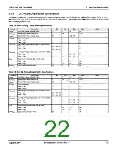
3.3.7
DC Analog PSoC Block Specifications
The following table lists guaranteed maximum and minimum specifications for the voltage and temperature ranges: 4.75V to 5.25V
and -40°C ≤ TA ≤ 85°C, or 3.0V to 3.6V and -40°C ≤ TA ≤ 85°C, respectively. Typical parameters apply to 5V and 3.3V at 25°C and
are for design guidance only.
Table 3-15. DC Analog PSoC Block Specifications
Symbol
RCT
Description
Min
Typ
12.2
80
Max
Units
kΩ
fF
Notes
Resistor Unit Value (Continuous Time)
–
–
–
–
CSC
Capacitor Unit Value (Switch Cap)
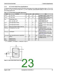
3.3.8
DC POR and LVD Specifications
The following table lists guaranteed maximum and minimum specifications for the voltage and temperature ranges: 4.75V to 5.25V
and -40°C ≤ TA ≤ 85°C, or 3.0V to 3.6V and -40°C ≤ TA ≤ 85°C, respectively. Typical parameters apply to 5V and 3.3V at 25°C and
are for design guidance only.
Note The bits PORLEV and VM in the table below refer to bits in the VLT_CR register. See the PSoC Mixed Signal Array Technical
Reference Manual for more information on the VLT_CR register.
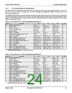
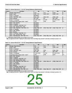
Table 3-16. DC POR and LVD Specifications
Symbol
Description
Min
Typ
Max
Units
Notes
Vdd Value for PPOR Trip (positive ramp)
PORLEV[1:0] = 00b
VPPOR0R
VPPOR1R
VPPOR2R
2.91
V
V
V
PORLEV[1:0] = 01b
–
–
4.39
4.55
–
–
PORLEV[1:0] = 10b
Vdd Value for PPOR Trip (negative ramp)
PORLEV[1:0] = 00b
VPPOR0
VPPOR1
VPPOR2
2.82
4.39
4.55
V
V
V
PORLEV[1:0] = 01b
PORLEV[1:0] = 10b
PPOR Hysteresis
PORLEV[1:0] = 00b
PORLEV[1:0] = 01b
PORLEV[1:0] = 10b
VPH0
VPH1
VPH2
–
–
–
92
0
–
–
–
mV
mV
mV
0
Vdd Value for LVD Trip
VM[2:0] = 000b
VM[2:0] = 001b
VM[2:0] = 010b
VM[2:0] = 011b
VM[2:0] = 100b
VM[2:0] = 101b
VM[2:0] = 110b
VM[2:0] = 111b
VLVD0
VLVD1
VLVD2
VLVD3
VLVD4
VLVD5
VLVD6
VLVD7
V
2.86
2.96
3.07
3.92
4.39
4.55
4.63
4.72
2.92
3.02
3.13
4.00
4.48
4.64
4.73
4.81
2.98a
3.08
3.20
4.08
4.57
V
V
V
V
V
V
V
V
4.74b
4.82
4.91
Vdd Value for PUMP Trip
VM[2:0] = 000b
VM[2:0] = 001b
VM[2:0] = 010b
VM[2:0] = 011b
VM[2:0] = 100b
VM[2:0] = 101b
VM[2:0] = 110b
VM[2:0] = 111b
VPUMP0
VPUMP1
VPUMP2
VPUMP3
VPUMP4
VPUMP5
VPUMP6
VPUMP7
V
V
V
V
V
V
V
V
V
2.96
3.03
3.18
4.11
4.55
4.63
4.72
4.90
3.02
3.10
3.25
4.19
4.64
4.73
4.82
5.00
3.08
3.16
3.32
4.28
4.74
4.82
4.91
5.10
a. Always greater than 50 mV above PPOR (PORLEV = 00) for falling supply.
b. Always greater than 50 mV above PPOR (PORLEV = 10) for falling supply.
August 3, 2004
Document No. 38-12012 Rev. *I
26

 CYPRESS [ CYPRESS ]